Method and structure of three-dimensional chip stacking

A technology of interconnect structure and die, which is applied in semiconductor/solid-state device components, semiconductor devices, electrical components, etc., and can solve problems such as complex design, increased circuit power consumption, and increased number and length of interconnects

Active Publication Date: 2017-07-14
TAIWAN SEMICON MFG CO LTD
View PDF7 Cites 22 Cited by
  • Summary
  • Abstract
  • Description
  • Claims
  • Application Information

AI Technical Summary

Problems solved by technology

In addition, when multiple devices are put into one chip, more complex designs are required
[0004] As the number of devices increases, an additional constraint comes from a significant increase in the number and length of interconnects between devices
When the number and length of interconnects increase, the circuit RC and power dissipation increase

Method used


Image

  • Method and structure of three-dimensional chip stacking
  • Method and structure of three-dimensional chip stacking
  • Method and structure of three-dimensional chip stacking

Examples


Embodiment Construction

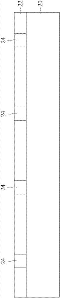
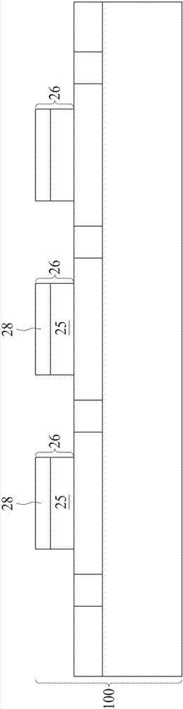
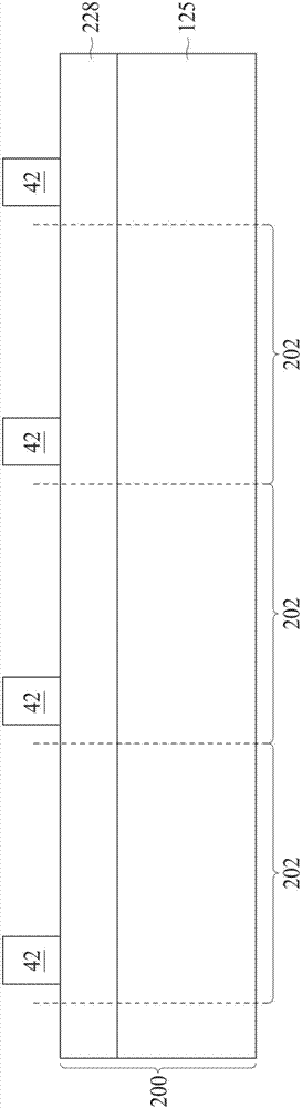
[0018] The following disclosure provides many different embodiments or examples for implementing different features of the presented subject matter. Specific examples of components and arrangements are described below to simplify the present disclosure. Of course, these are examples only and are not intended to limit the invention. For example, in the following description, forming a first component over or on a second component may include embodiments in which the first component and the second component are formed in direct contact, and may also include embodiments in which the first component and the second component may be formed in direct contact. An embodiment in which an additional part is formed so that the first part and the second part may not be in direct contact. In addition, the present invention may repeat reference numerals and / or letters in various instances. This repetition is for the sake of simplicity and clarity and does not in itself indicate a relations...


PUM


Abstract

A method includes placing a first plurality of device dies over a first carrier, with the first plurality of device dies and the first carrier in combination forming a first composite wafer. The first composite wafer is bonded to a second wafer, and the first plurality of device dies is bonded to a second plurality of device dies in the second wafer through hybrid bonding. The method further includes de-bonding the first carrier from the first plurality of device dies, encapsulating the first plurality of device dies in an encapsulating material, and forming an interconnect structure over the first plurality of device dies and the encapsulating material. The embodiment of the invention relates to a package and a manufacturing method thereof.

Description

technical field [0001] Embodiments of the present invention relate to a package and a manufacturing method thereof. Background technique [0002] Since the invention of the integrated circuit, the semiconductor industry has experienced continuous rapid growth due to the increasing integration of various electronic components (i.e., transistors, diodes, resistors, capacitors, etc.). In most cases, this improvement in integration comes from iterative reductions in minimum feature size, which allow more components to fit into a given area. [0003] These integration improvements are essentially two-dimensional (2D) in nature, since the volume occupied by the integrated components is located substantially on the surface of the semiconductor wafer. Although dramatic improvements in lithography have led to significant improvements in 2D integrated circuit formation, there are physical limits to the densities that can be achieved in two dimensions. One of these constraints is the...

Claims


Application Information

Patent Timeline
Patent Type & Authority Applications(China)
IPC IPC(8): H01L21/60H01L23/52H01L23/538H01L21/56H01L23/31
CPCH01L21/56H01L23/31H01L23/52H01L23/538H01L24/09H01L2224/091H01L2224/04105H01L2224/12105H01L2224/32225H01L2224/73267H01L2224/92244H01L21/568H01L24/19H01L24/20H01L2224/24137H01L2224/32145H01L2924/18162H01L2224/80132H01L2224/214H01L23/3128H01L23/5389H01L21/6835H01L24/80H01L24/94H01L24/96H01L24/97H01L2221/68345H01L2221/68359H01L2224/08145H01L2224/80006H01L2224/80895H01L2224/80896H01L2224/94H01L2224/96H01L2224/97H01L2924/1431H01L2924/1434H01L2924/1816H01L2224/8014H01L2924/00014H01L2224/08121H01L2224/05571H01L2224/08111H01L21/486H01L23/49827H01L2224/80H01L2224/83H01L2224/29099H01L25/50H01L25/0652H01L21/4853H01L23/3157
Inventor 余振华林咏淇邱文智
Owner TAIWAN SEMICON MFG CO LTD
Why Eureka
Try Eureka