Array substrate and display panel

An array substrate and display area technology, applied in static indicators, nonlinear optics, instruments, etc., can solve the problem of inability to realize a narrow frame of an array substrate, and achieve the effect of reducing the width of the frame

Active Publication Date: 2017-09-26
XIAMEN TIANMA MICRO ELECTRONICS
View PDF4 Cites 35 Cited by
  • Summary
  • Abstract
  • Description
  • Claims
  • Application Information

AI Technical Summary

Problems solved by technology

At this time, the shift register unit 005 and the electrostatic protection circuit 006 are arranged in the non-linear area 003 of ...

Method used


Image

  • Array substrate and display panel
  • Array substrate and display panel
  • Array substrate and display panel

Examples


Embodiment Construction

[0031] In order to make the above objects, features and advantages of the present application more obvious and comprehensible, the present application will be further described below in conjunction with the accompanying drawings and embodiments.

[0032] It should be noted that specific details are set forth in the following description to facilitate a full understanding of the present application. However, the present application can be implemented in many other ways different from those described here, and those skilled in the art can make similar promotions without departing from the connotation of the present application. The present application is therefore not limited by the specific embodiments disclosed below.

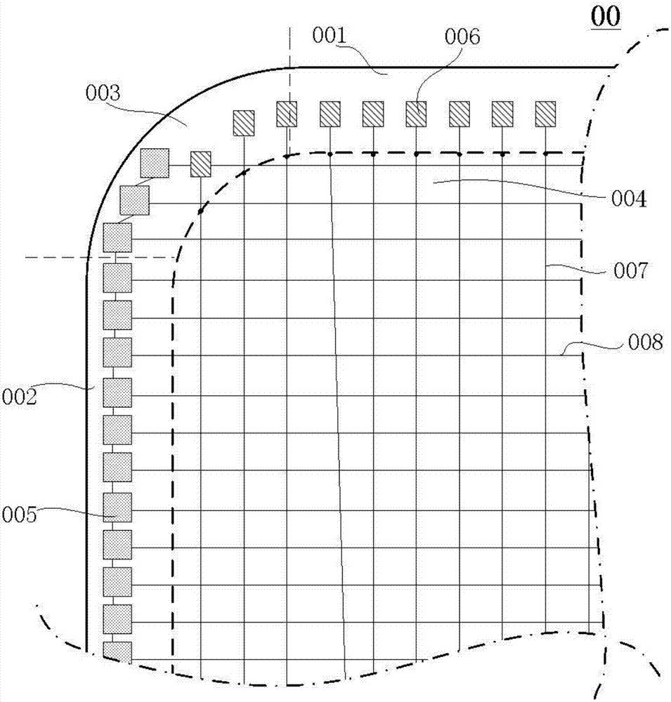
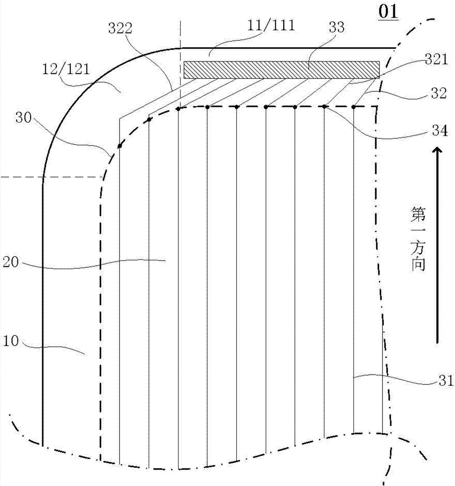
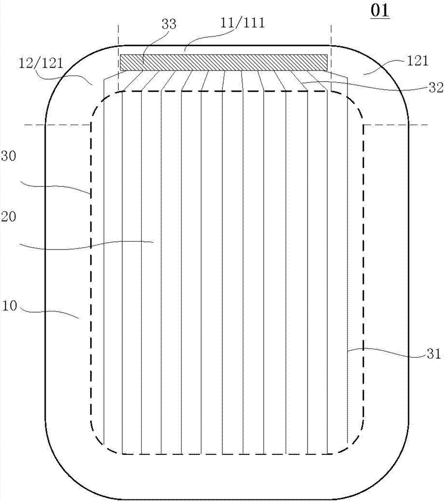
[0033] Please refer to figure 2 , figure 2 is a partial schematic diagram of an array substrate according to an embodiment of the present invention. The array substrate 01 provided by the present invention is a non-rectangular array substrate. Optionally, ...


PUM


Abstract

The invention provides an array substrate and a display panel comprising the array substrate. The array substrate is a non-rectangular array substrate and comprises a display area and a non-display area surrounding the display area; the non-display area comprises a first linear area and a first non-linear area connected with the first linear area, and the first linear area and the display area are arranged in the first direction; the display area comprises a plurality of signal lines extending in the first direction; the non-display area comprises a plurality of signal connecting lines; the first linear area comprises a signal control circuit; the signal connecting lines are connected with the signal lines and the signal control circuit, wherein the signal connecting lines comprise first signal connecting lines only extending in the first linear area and second signal connecting lines extending from the first linear area to the first non-linear area. According to the array substrate and the display panel, a voltage signal provided by the signal control circuit can be normally received by the signal lines, and the border width of the first non-linear area can be decreased, so that the border width of the linear area is decreased.

Description

technical field [0001] The present invention relates to the display field, in particular to an array substrate and a display panel including the array substrate. Background technique [0002] Today, special-shaped display devices such as wearable displays, vehicle dashboards, and full screens have become a hot spot in the display field. Taking a liquid crystal display device as an example for illustration, when the liquid crystal display device is designed to have a special shape, correspondingly, the array substrate included in the liquid crystal display device is also a special shape, such as figure 1 as shown, figure 1 It is a partial schematic diagram of an array substrate in the prior art. [0003] The array substrate 00 includes a display area 004 and a non-display area surrounding the display area 004, wherein the non-display area includes linear areas 001, 002 and non-linear areas 003, from figure 1 It can be seen from the figure that the outer contours of the arr...

Claims


Application Information

Patent Timeline
IPC IPC(8): G02F1/1362G02F1/133
CPCG02F1/13306G02F1/136286
Inventor 吴晓晓刘冰萍陈国照
Owner XIAMEN TIANMA MICRO ELECTRONICS
Why Eureka
Try Eureka