Touch electrode structure, touch screen panel and display device

A technology of touch electrodes and touch screens, which is applied in the fields of electrical digital data processing, instruments, calculations, etc., can solve the problems of large area occupied by touch detection chips, unfavorable design of narrow borders of touch screens, and high production cost of touch screens. The effect of reducing the number, reducing the frame width, and increasing the aperture ratio

Active Publication Date: 2015-11-25
BOE TECH GRP CO LTD +1
View PDF3 Cites 24 Cited by
  • Summary
  • Abstract
  • Description
  • Claims
  • Application Information

AI Technical Summary

Problems solved by technology

[0004] In the above-mentioned self-capacitance sensing touch screen, in order to ensure the touch accuracy, a large number of self-capacitance electrodes are generally set, and accordingly, the number of wires will also be large. The number of traces will also be large, which is not conducive to the design of the narrow frame of the touch screen; and the number of terminals used to connect the peripheral traces in the touch detection chip will also be large, which will make the touch detection chip The measurement chip occupies a large area, which in turn will increase the production cost of the touch screen; in addition, in the production process of the above touch screen, in order not to increase the number of masks, the wires and data lines are generally arranged side by side on the same layer, which will inevitably affect Aperture ratio of touch screen

Method used


Image

  • Touch electrode structure, touch screen panel and display device
  • Touch electrode structure, touch screen panel and display device
  • Touch electrode structure, touch screen panel and display device

Examples


Embodiment Construction

[0027] The specific implementation manners of the touch electrode structure, touch screen and display device provided by the embodiments of the present invention will be described in detail below with reference to the accompanying drawings.

[0028] The shapes and sizes of the components in the drawings do not reflect their true proportions, but are only intended to schematically illustrate the content of the present invention.

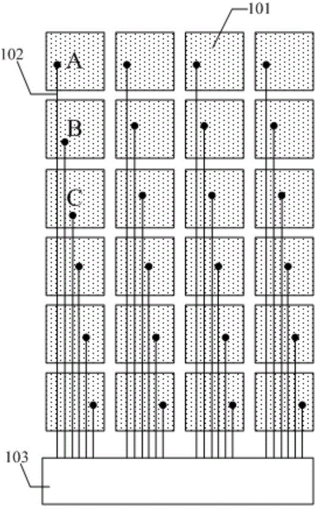
[0029] A touch electrode structure provided by an embodiment of the present invention, such as image 3 As shown, including: a plurality of self-capacitance electrode groups arranged in a matrix (such as image 3 As shown in the dashed box, image 3 2 rows×4 columns of self-capacitance electrode groups are shown); wherein,

[0030] Each self-capacitance electrode group includes two L-shaped self-capacitance electrodes 1 that are insulated from each other and arranged complementary.

[0031] The above-mentioned touch electrode structure provided by ...


PUM


Abstract

The invention discloses a touch electrode structure, a touch screen panel and a display device. The touch electrode structure comprises multiple self-capacitance electrode groups arranged in a matrix shape, wherein each self-capacitance electrode group comprises two L-shaped self-capacitance electrodes which are insulated mutually and complement each other, that is, existing three rectangular and parallel self-capacitance electrodes are combined into the two L-shaped self-capacitance electrodes which complement each other under the premise that the touch precision is unchanged, thus, under the premise that the touch precision of the touch screen panel is guaranteed, the number of the self-capacitance electrodes can be reduced, the number of leads which are connected with the self-capacitance electrodes in the one-to-one correspondence manner can be reduced correspondingly, the opening ratio of the touch screen panel can be increased, besides, the number of peripheral wires connected with the leads in the one-to-one correspondence manner can be reduced, the frame width of the touch screen panel can be reduced, in addition, the number of wiring terminals for connecting the peripheral wires in a touch detection chip can be reduced, and the area occupied by the touch detection chip can be reduced.

Description

technical field [0001] The present invention relates to the field of display technology, in particular to a touch electrode structure, a touch screen and a display device. Background technique [0002] With the rapid development of display technology, touch screens (TouchScreenPanel) have gradually spread in people's lives. According to the principle, touch screens can be divided into capacitive sensing touch screens, resistive sensing touch screens and optical sensing touch screens, etc. Among them, capacitive sensing touch screens include self-capacitance sensing touch screens and mutual capacitance sensing touch screens. Compared with the mutual capacitance sensing touch screen, the self-capacitance sensing touch screen has a higher signal-to-noise ratio and higher accuracy of touch sensing. [0003] In the existing self-capacitance sensing touch screen, such as figure 1 As shown, there are a plurality of self-capacitance electrodes 101 arranged on the same layer and in...

Claims


Application Information

Patent Timeline
Patent Type & Authority Applications(China)
IPC IPC(8): G06F3/044
Inventor 龙跃冯远明刘庭良
Owner BOE TECH GRP CO LTD
Why Eureka
Try Eureka