Supercharge Your Innovation With Domain-Expert AI Agents!

semiconductor manufacturing method

A manufacturing method and semiconductor technology, applied in semiconductor devices, semiconductor/solid-state device parts, electric solid-state devices, etc., can solve problems such as uneven stress distribution, reflecting the overlay position of the cell array area, overlay alignment deviation, etc.

Active Publication Date: 2018-12-14
YANGTZE MEMORY TECH CO LTD
View PDF9 Cites 0 Cited by
  • Summary
  • Abstract
  • Description
  • Claims
  • Application Information

AI Technical Summary

Problems solved by technology

[0011] As we all know, the cell array area is the core component of 3D NAND, but its position is far away from the OVL mark in the scribing tape; the device density of the 3D NAND cell array area and the number of stacked layers (the two are also the so-called "weight (weight) , W)") is quite different from the dicing zone area, that is, the weight of the cell array area is larger and the weight of the dicing zone area is relatively small, so the stress distribution of the wafer is also quite different, which will cause stress Overlay alignment deviation caused by uneven distribution; and the OVL mark located in the scribe tape is difficult to accurately reflect the overlay position of the cell array area

Method used


Image

  • semiconductor manufacturing method
  • semiconductor manufacturing method
  • semiconductor manufacturing method

Examples


Embodiment Construction

[0034] Exemplary embodiments of the present disclosure will be described in more detail below with reference to the accompanying drawings. Although exemplary embodiments of the present disclosure are shown in the drawings, it should be understood that the present disclosure may be embodied in various forms and should not be limited by the embodiments set forth herein. Rather, these embodiments are provided for more thorough understanding of the present disclosure and to fully convey the scope of the present disclosure to those skilled in the art.

[0035] According to an embodiment of the present invention, a method for overlay alignment (OVL) in a semiconductor manufacturing process is proposed.

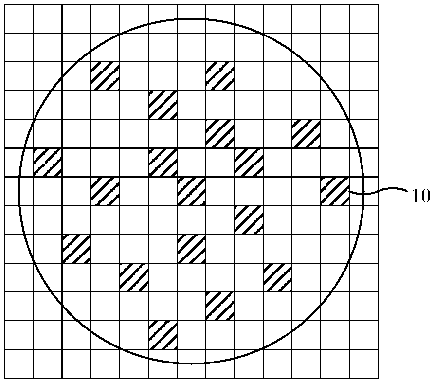
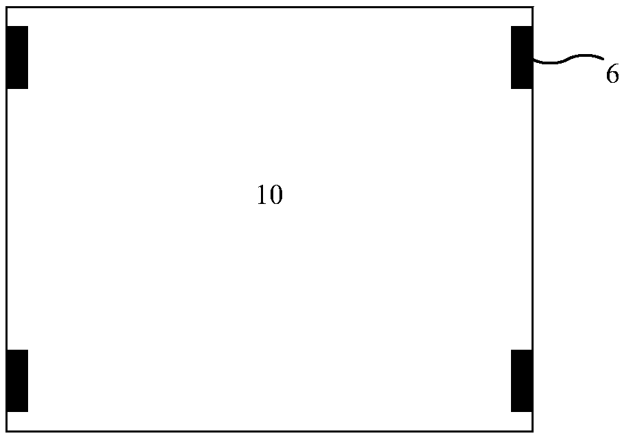
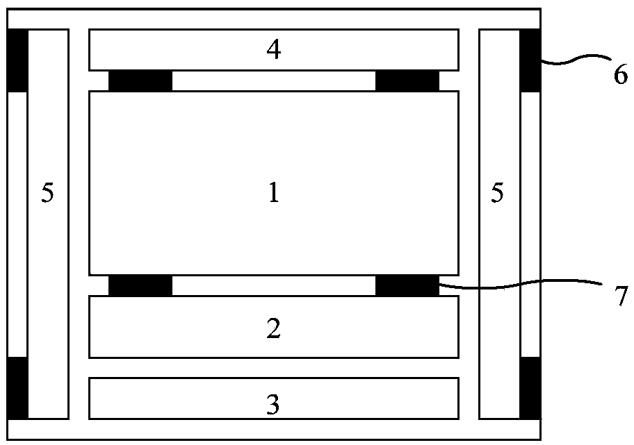
[0036] Firstly, two sets of overlay alignment (OVL) marks at different positions are set in each exposure area, that is, the OVL marks in the cell array area and the OVL marks in the scribe tape. Wherein the cell array area OVL mark 7 is close to the cell array area 1 and is locate...


PUM


Abstract

The present invention provides a semiconductor manufacturing method for performing an overlay alignment (OVL) operation, wherein an OVL mark is arranged in a 3D NAND cell array area and a scribe band, that is, the cell array area OVL and the scribe band OVL are set, Directly measure the deviation of the OVL mark, and through two separate data fittings, and give different weights, it can more accurately reflect the overlay alignment of the cell array area, and overcome the existing problem of only relying on the OVL mark in the dicing tape It is difficult to reflect the defect of accurate overlay position.

Description

technical field [0001] The invention relates to the field of semiconductor manufacturing methods, in particular to an overlay alignment (OVL, Overlayer) method in 3D NAND manufacturing. Background technique [0002] 3D NAND is currently a popular device in the field of semiconductor memory. It adopts a device structure of vertically stacking multi-layer memory cells, which reduces the unit cost of memory cells while achieving extremely high data storage density. Due to the need for multi-layer stacking in the process, which involves multi-layer photolithography and alignment processes, if the overlay alignment accuracy cannot meet the device requirements, it will cause process failure and device yield reduction, resulting in cost increase unnecessarily. [0003] At present, the conventional overlay alignment process in the 3D NAND manufacturing process includes: [0004] Measure multiple exposure areas (Shot) 10 distributed on the wafer (ie attached figure 1 The shaded sq...

Claims


Application Information

Patent Timeline
Patent Type & Authority Patents(China)
IPC IPC(8): H01L23/544H01L27/11551H01L27/11578H10B41/20H10B43/20
CPCH01L23/544H01L2223/54426H10B41/20H10B43/20
Inventor 杨要华刘藩东何佳夏志良霍宗亮冯耀斌
Owner YANGTZE MEMORY TECH CO LTD
Features
  • R&D
  • Intellectual Property
  • Life Sciences
  • Materials
  • Tech Scout
  • Unparalleled Data Quality
  • Higher Quality Content
  • 60% Fewer Hallucinations
Learn More