
Advanced processing control for technology sensing dimension target

A technology with process and target characteristics, applied in the field of advanced process control, which can solve the problems that the adjustment of process specifications is not optimal, and the characteristics cannot be represented.

Inactive Publication Date: 2018-01-12
GLOBALFOUNDRIES U S INC MALTA
View PDF5 Cites 0 Cited by
  • Summary
  • Abstract
  • Description
  • Claims
  • Application Information

AI Technical Summary

Problems solved by technology

Unfortunately, when the total number of features is high (e.g., hundreds), such a small sample mean may not represent most of the features, making process specification adjustments based on this mean suboptimal

Method used


Image

  • Advanced processing control for technology sensing dimension target
  • Advanced processing control for technology sensing dimension target
  • Advanced processing control for technology sensing dimension target

Examples


Embodiment Construction

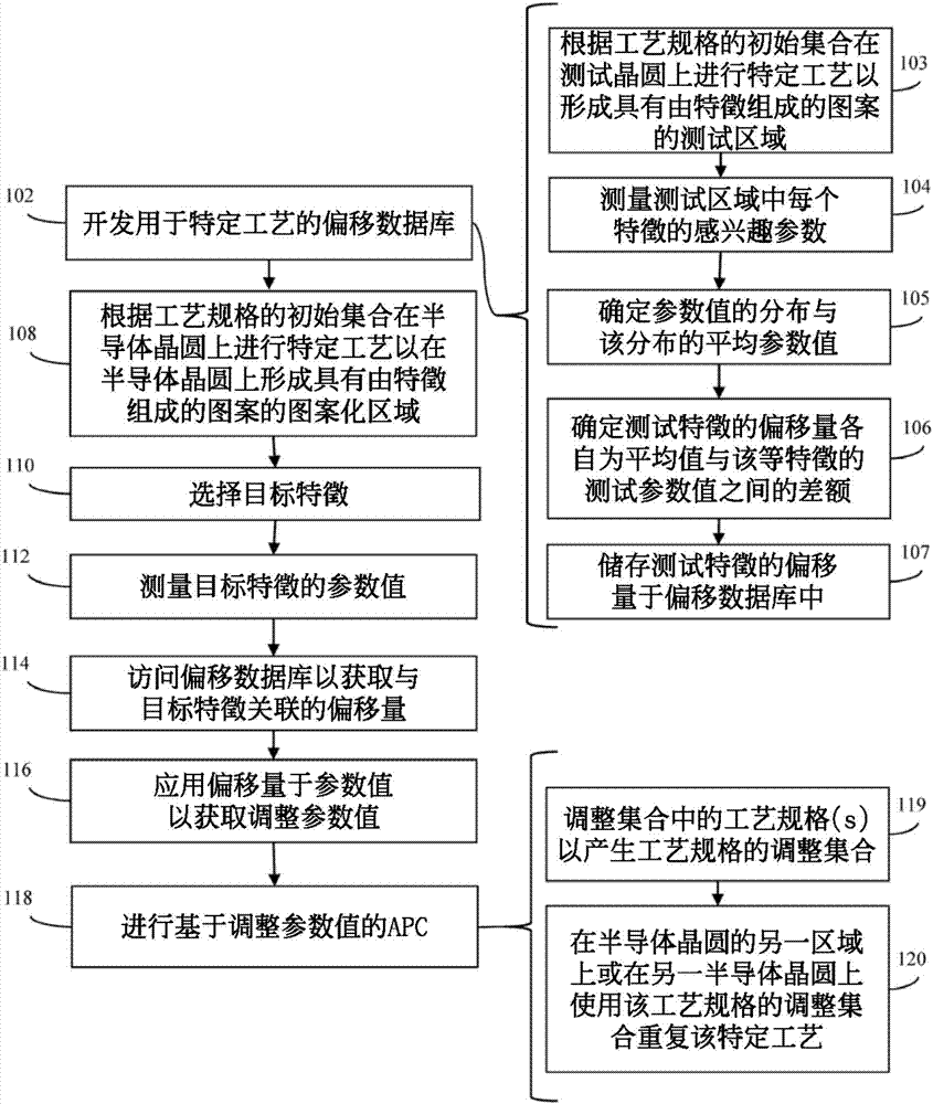
[0022] As mentioned above, in semiconductor wafer processing, advanced process control (APC) refers to the selective adjustment of one or more process specifications of a particular process based on feedback so that the process can be repeated on the same semiconductor wafer or on different semiconductor wafers. At a particular process, the target parameter value for each of its multiple instances is achieved for the same feature in the pattern. For example, certain processes (eg, photolithography or etching processes) used to form a patterned region on a semiconductor wafer with a pattern of several features (eg, more than 200 features) can perform APC. In particular, APC may be performed when attempting to achieve target parameter values ​​in each of the characteristics. For example, the target parameter value may be a key dimension. For purposes of this disclosure, the term "key dimension" refers to the minimum dimension of a feature (eg, the minimum width of a feature). ...


PUM


Abstract

The invention relates to an advanced processing control for technology sensing dimension target, which discloses a plurality of advanced processing control (APC) methods for specific technology. The specific technology (e.g. photoetching or etching technology) is conducted on wafer to establish patterns formed by features. The parameter of the target features is measured and the parameter value isapplied in the APC. The APC is conducted based on adjusted parameter value but not the actual parameter value. Concretely speaking, an offset amount is applied to the actual parameter value to obtainthe adjusted parameter value, which is more suitable for representing most features of the patterns.

Description

technical field [0001] The present invention relates to advanced process control (APC), and more particularly to an advanced process control (APC) method for a specific process to minimize dimension variation. Background technique [0002] In semiconductor wafer processing, advanced process control (APC) refers to selectively adjusting one or more process specifications of a particular process based on feedback so that the particular process can be repeated on the same semiconductor wafer or on different semiconductor wafers. , achieving the target parameter value for each of its multiple instances for the same feature in a pattern. For example, certain processes (eg, photolithography or etching processes) used to form a patterned region on a semiconductor wafer with a pattern of several features (eg, more than 200 features) can perform APC. In particular, APC may be performed when attempting to achieve target parameter values ​​in each of the characteristics. For example,...

Claims


Application Information

Patent Timeline
IPC IPC(8): H01L21/66G06K9/20
CPCG03F7/70525G03F7/70625H01L22/12G05B2219/45031G05B19/0426H01L22/20G06F16/245G03F1/70G03F7/20G05B17/02H01L21/0274H01L21/30604H01L21/308
Inventor P·亚申斯基F·卡伦贝格S·克兰普R·席翁R·泽尔特曼
Owner GLOBALFOUNDRIES U S INC MALTA
Learn More