Array substrate and production method thereof and touch display panel
An array substrate and array technology, applied in nonlinear optics, instruments, optics, etc., can solve the problems of a large number of touch wiring and occupying a large wiring area, and achieve the effects of reducing production costs, reducing quantity, and narrowing width
- Summary
- Abstract
- Description
- Claims
- Application Information
AI Technical Summary
Problems solved by technology
Method used
Image


Examples
Embodiment Construction
[0025] The following will clearly and completely describe the technical solutions in the embodiments of the present invention with reference to the drawings in the embodiments of the present invention. Wherein, the accompanying drawings are only used for exemplary illustration, and represent only schematic diagrams, and should not be understood as limitations on this patent.
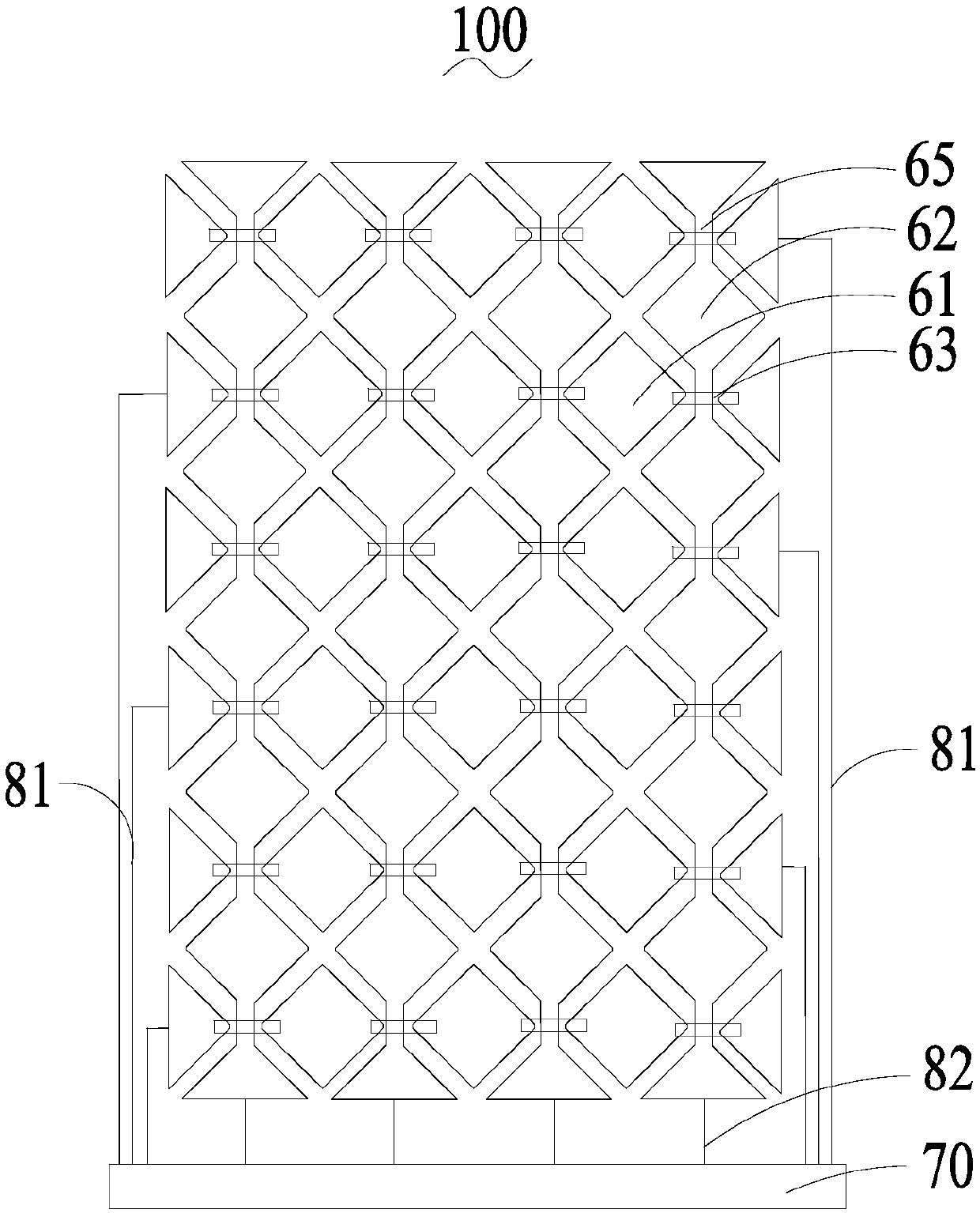
[0026] see figure 1 and image 3 , the present invention provides an array substrate 100 . The array substrate 100 includes a substrate 10 , a thin film transistor disposed on the substrate, and a flat layer 30 covering the thin film transistor. A touch layer 60 is disposed on a side of the planar layer 30 away from the thin film transistor. The touch layer 60 includes a plurality of touch electrodes, and the plurality of touch electrodes are electrically connected to a touch chip 70, thereby realizing the touch control through the touch layer 60 and the touch chip 70. The touch function of the contr...
PUM
 Abstract
Description
Claims
Application Information