Supercharge Your Innovation With Domain-Expert AI Agents!

Substrate processing equipment

A substrate processing device and technology for substrates, which are applied in the manufacturing of electrical components, circuits, semiconductor/solid-state devices, etc., can solve the problems of easy residual processing liquid and increased residual processing liquid.

Active Publication Date: 2021-02-26
DAINIPPON SCREEN MTG CO LTD
View PDF6 Cites 0 Cited by
  • Summary
  • Abstract
  • Description
  • Claims
  • Application Information

AI Technical Summary

Problems solved by technology

However, in this jig pin, the treatment liquid tends to remain between the conductive member and the pin cover.
In particular, since the pin cover covers substantially the entire area of ​​the conductive member, the remaining amount of the treatment liquid increases

Method used


Image

  • Substrate processing equipment
  • Substrate processing equipment
  • Substrate processing equipment

Examples


Embodiment approach

[0109] The present invention is not limited to the contents of the above-described embodiments, and various changes can be made within the scope of the present invention.

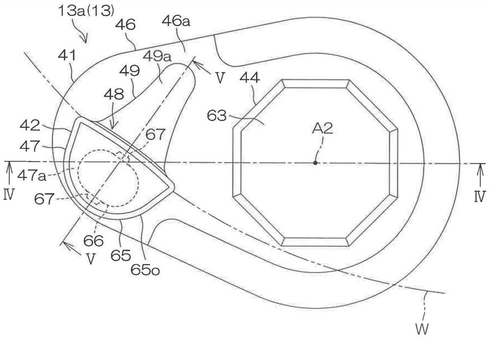
[0110] For example, in the above-mentioned embodiment, the case where the jig cover 42 covers the entire area of ​​the top surface 47 a of the contact portion 47 in a plan view has been described, but a part of the top surface 47 a of the contact portion 47 may be exposed from the jig cover 42 in a plan view. .

[0111] In the above-mentioned embodiment, the case where the lower surface 65d of the cover portion 65 is spaced upward from the top surface 47a of the contact portion 47 and the gap G1 is formed between the conductive member 41 and the jig cover 42 has been described. However, the cover portion 65 The lower surface 65d of the contact portion 47 may also be in contact with the top surface 47a.

[0112] In the above-mentioned embodiment, the case where the jig cover 42 is attached to the conductive...


PUM


Abstract

The present invention provides a substrate processing apparatus, comprising: a plurality of clamp members (13), which hold the substrate in a horizontal posture by clamping the substrate to be horizontal; a processing liquid supply unit, which supplies the processing liquid to the substrate (W) ; and a heat source disposed above the substrate. The jig member (13) includes: a conductive member (41), at least a part of which is formed of a material containing carbon, including: a base portion (46) disposed below the substrate (W); and a contact portion (47), Protrude upward from the upper surface (46a) of the above-mentioned base part (46), and press against the outer peripheral part of the substrate (W); and the jig cover (42), which is attached to the conductive member (41), does not cover the base part ( 46) to cover the contact portion (47).

Description

technical field [0001] The present invention relates to a substrate processing device for processing a substrate. The substrates to be processed include, for example, semiconductor wafers, substrates for liquid crystal display devices, substrates for plasma displays, substrates for FED (Field Emission Display: field emission displays), substrates for optical disks, substrates for magnetic disks, substrates for magneto-optical disks, and optical disks. Mask substrates, ceramic substrates, solar cell substrates, etc. Background technique [0002] In a manufacturing process of a semiconductor device, a liquid crystal display device, etc., a substrate processing apparatus for processing a substrate such as a semiconductor wafer or a glass substrate for a liquid crystal display device is used. Japanese Unexamined Patent Application Publication No. 2014-241390 discloses a sheet-type substrate processing apparatus that processes sheets one by one. [0003] This substrate processi...

Claims


Application Information

Patent Timeline
Patent Type & Authority Patents(China)
IPC IPC(8): H01L21/67H01L21/687
CPCH01L21/67023H01L21/67115H01L21/68714H01L21/6704H01L21/6715H01L21/6875H01L21/68764
Inventor 岩田敬次岩见优树小林知之天久贤治佐藤昌治
Owner DAINIPPON SCREEN MTG CO LTD
Features
  • R&D
  • Intellectual Property
  • Life Sciences
  • Materials
  • Tech Scout
  • Unparalleled Data Quality
  • Higher Quality Content
  • 60% Fewer Hallucinations
Learn More