
Improved epitaxial growth between gates

A technology of electrostatic discharge and devices, which is applied in the field of electrostatic discharge devices and their formation, and can solve problems such as damage

Active Publication Date: 2018-03-20
TAIWAN SEMICON MFG CO LTD
View PDF3 Cites 1 Cited by
  • Summary
  • Abstract
  • Description
  • Claims
  • Application Information

AI Technical Summary

Problems solved by technology

If a silicide layer forms there, the current flowing through the source and drain regions will tend to move primarily through the silicide, which can lead to damage as the current density created by the high ESD currents can burn off the silicide and surrounding s material
[0005] Another problem related to forming ESD devices arises when the source and drain regions are formed by an epitaxial growth process

Method used


Image

  • Improved epitaxial growth between gates
  • Improved epitaxial growth between gates
  • Improved epitaxial growth between gates

Examples


Embodiment Construction

[0025] It should be appreciated that the following disclosure provides many different embodiments or examples for implementing different features of the invention. Specific examples of components and arrangements are described below to simplify the present disclosure. Of course, these are examples only and are not intended to limit the invention. In addition, in the subsequent description, performing the first process before the second process may include an embodiment in which the second process is performed immediately after the first process, and may also include an example in which an additional process may be performed between the first process and the second process. Example of process. The various figures may be arbitrarily drawn in different scales for simplicity and clarity. In addition, in the following description, forming the first part over or on the second part may include an embodiment in which the first part and the second part are formed in direct contact, a...


PUM


Abstract

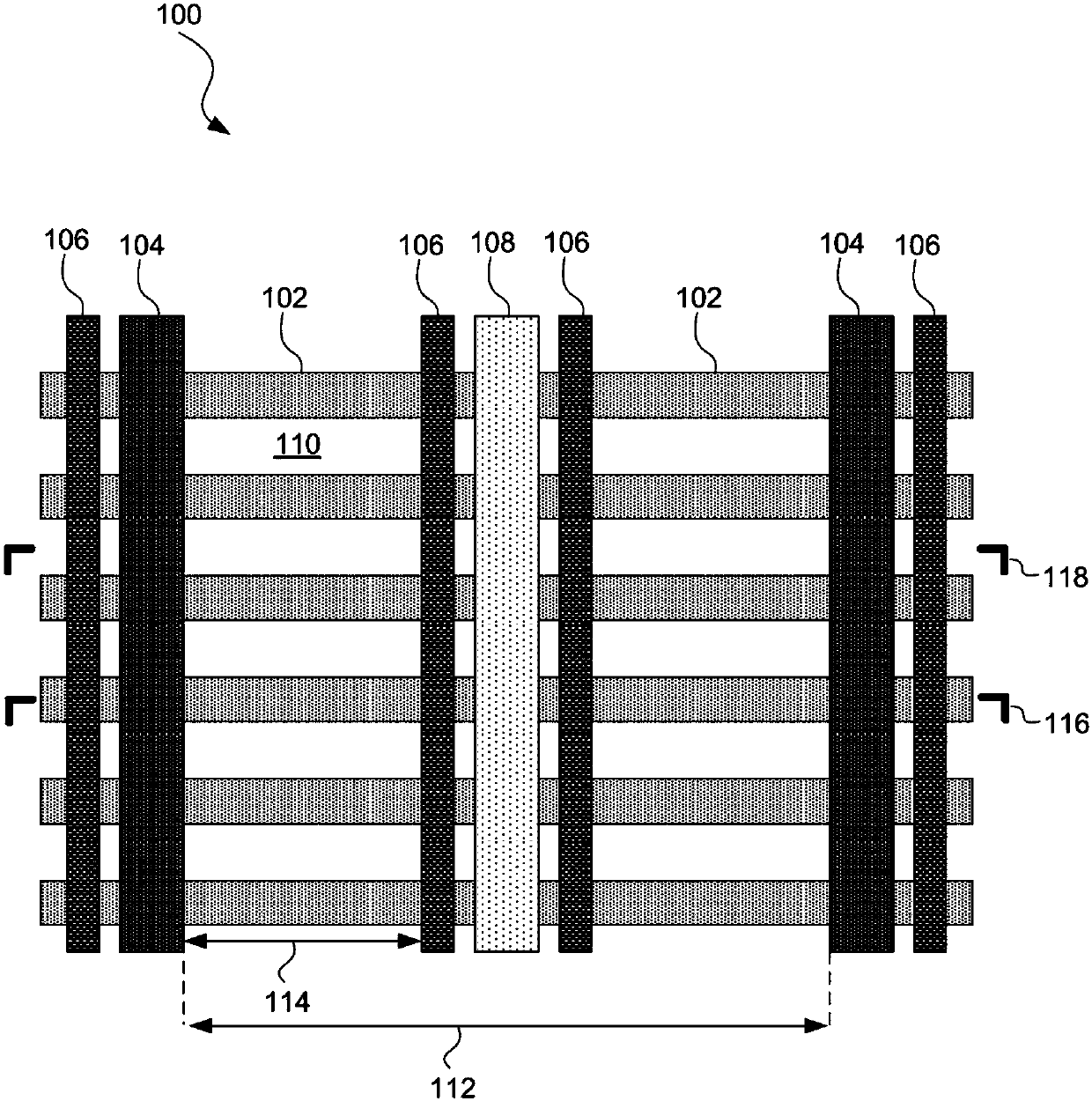
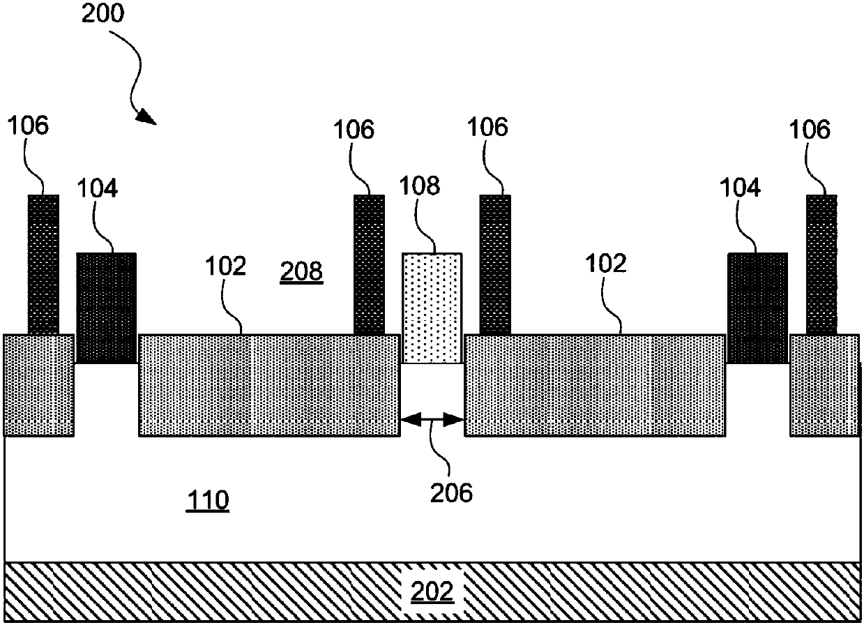
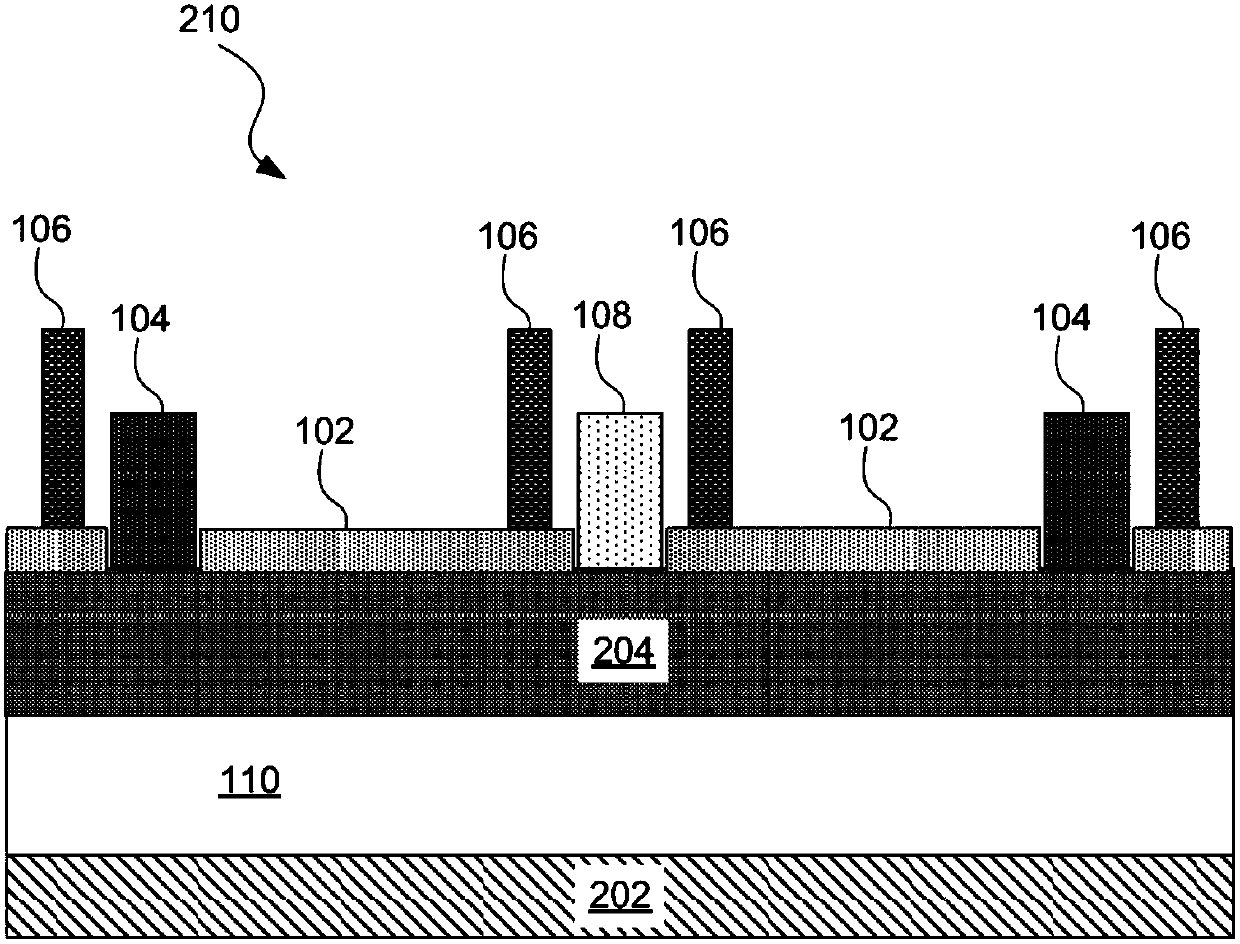
An integrated circuit device includes at least two epitaxially grown active regions grown onto a substrate, the active regions being placed between a first gate device and a second gate device. The integrated circuit device includes at least one dummy gate between the two epitaxially grown active regions and between the first gate device and the second gate device, wherein each active region is substantially uniform in length. The first gate device and the second device are formed over a first well having a first conductivity type and the dummy gate is formed over a second well having a secondconductivity type. The invention also provides a method of forming an electrostatic discharge (ESD) device.

Description

technical field [0001] Embodiments of the present invention generally relate to the field of semiconductors, and more particularly, to electrostatic discharge devices and methods of forming the same. Background technique [0002] Electronic devices utilizing integrated circuits are susceptible to electrostatic discharge (ESD). Electrostatic discharge can occur from persons handling the device or from other sources. Electrostatic discharge can damage circuits by passing large amounts of current through circuits sensitive to such high currents. To reduce susceptibility to ESD damage, integrated circuits often include ESD devices that keep ESD away from sensitive circuitry. [0003] One type of ESD device involves multiple active regions, such as source or drain regions, located between elongated gate devices. Gate devices are used for the gates of transistors. Transistors act as switches, activated when high currents such as ESD are detected. The activation switch allows ...

Claims


Application Information

Patent Timeline
IPC IPC(8): H01L27/02H01L21/77
CPCH01L21/77H01L27/0266H01L27/0285H01L21/823431H01L27/0886H01L29/66545H01L27/0207H01L27/105
Inventor 林文杰杨涵任苏郁迪
Owner TAIWAN SEMICON MFG CO LTD
Learn More