Polishing method and polishing device

A grinding method and technology of a grinding device, which are applied in the direction of grinding devices, grinding machine tools, and parts of grinding machine tools, can solve problems such as inability to eliminate film thickness and unevenness, and achieve the goal of eliminating film thickness unevenness and reducing film thickness differences Effect

Active Publication Date: 2018-05-11
EBARA CORP
View PDF11 Cites 3 Cited by
  • Summary
  • Abstract
  • Description
  • Claims
  • Application Information

AI Technical Summary

Problems solved by technology

However, conventional CMP technology cannot eliminate s

Method used


Image

  • Polishing method and polishing device
  • Polishing method and polishing device
  • Polishing method and polishing device

Examples


Embodiment Construction

[0081] Hereinafter, embodiments of the present invention will be described with reference to the drawings.

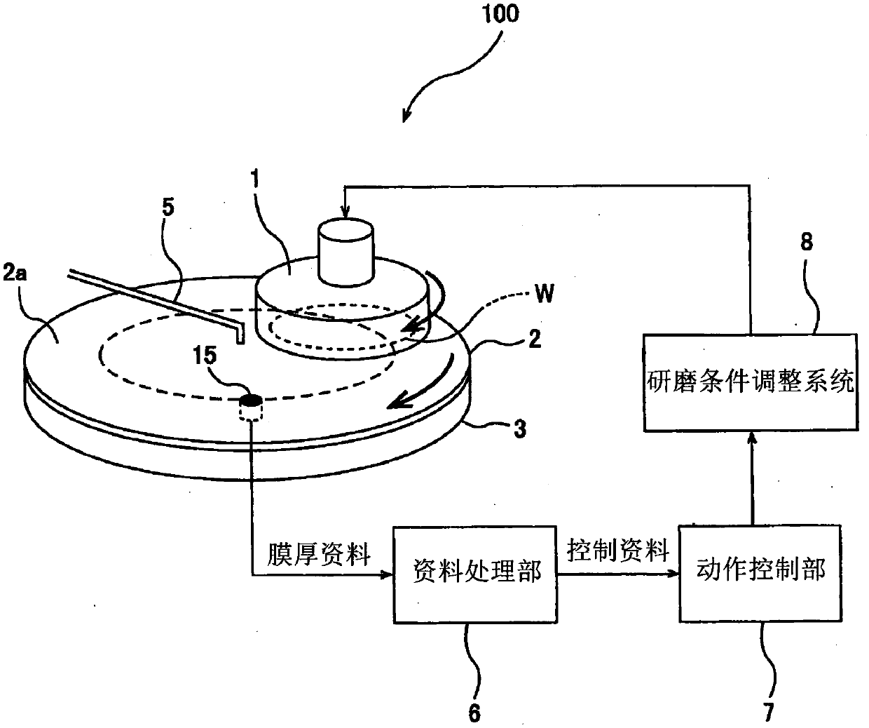
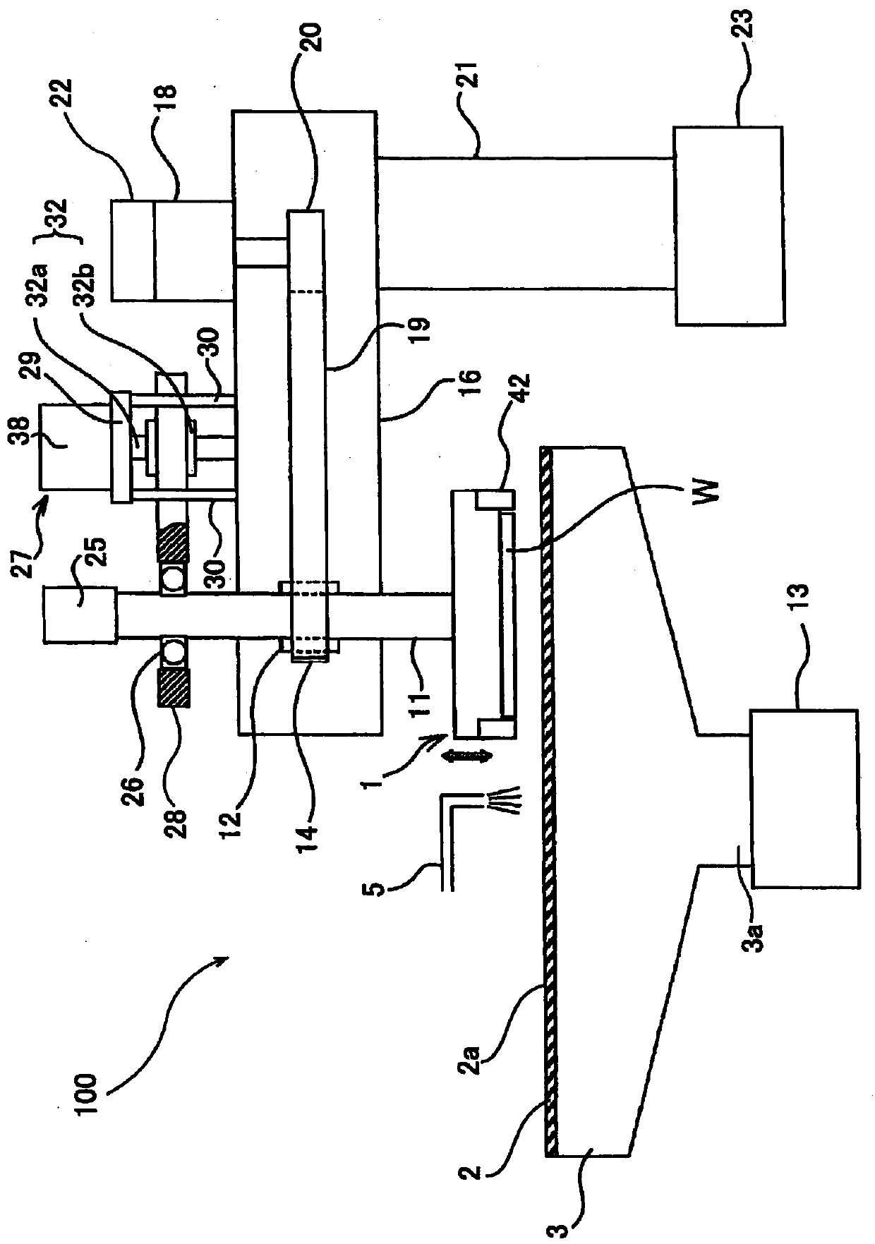
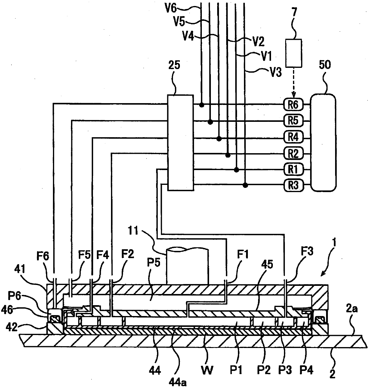
[0082] figure 1 It is a perspective view showing an embodiment of a CMP (Chemical Mechanical Polishing) apparatus which is a main polishing apparatus for chemically mechanically polishing the entire surface of a substrate such as a wafer. The CMP apparatus 100 as a main polishing apparatus includes: a polishing head (substrate holding device) 1 that holds and rotates a wafer W as an example of a substrate; a polishing table 3 that supports a polishing pad 2; and a slurry supply that supplies slurry to the polishing pad 2. Nozzle 5. The upper surface of the polishing pad 2 constitutes a polishing surface 2a for polishing the wafer W. As shown in FIG.

[0083] The polishing head 1 is configured to hold the wafer W on its lower surface by vacuum suction. The polishing head 1 and the polishing table 3 rotate in the same direction as indicated by arrows, and the polishing...


PUM


Abstract

The present invention relates to a method and a device for polishing the surface of a substrate having film thickness unevenness in the circumferential direction of the substrate. Disclosed is a polishing method whereby: film thickness distribution in the circumferential direction of a substrate (W) is acquired; a first region having the largest or smallest film thickness is determined on the basis of the film thickness distribution; a polishing table (3) holding a polishing pad (2) is rotated; the surface of the substrate (W) is pressed to the polishing pad (2), while rotating the substrate by means of a polishing head (1); and the first region is polished at a removing rate that is different from the removing rate for a second region within the surface of the substrate (W).

Description

technical field [0001] The invention relates to a grinding method and a grinding device for grinding the surface of a substrate such as a wafer, in particular to a method and a device for grinding a substrate surface with uneven film thickness along the circumferential direction of the substrate. Background technique [0002] Various films are formed on wafers in the manufacture of semiconductor elements. After the film forming process, the wafer is ground to remove unnecessary portions of the film and surface irregularities. Chemical mechanical polishing (CMP) is a representative technique of wafer polishing. This CMP is performed by supplying slurry on the polishing surface, while bringing the wafer into sliding contact with the polishing surface. The film formed on the wafer is polished by the combined effect of the mechanical action of the abrasive grains contained in the slurry and the chemical action of the chemical components of the slurry. [0003] prior art liter...

Claims


Application Information

Patent Timeline
IPC IPC(8): B24B37/005B24B37/30B24B37/34B24B49/04H01L21/304
CPCH01L22/12H01L22/20B24B37/013B24B37/32B24B49/105B24B49/12B24B37/042B24B37/107B24B37/005B24B37/30B24B37/34B24B49/04H01L21/304H01L21/30625H01L22/26
Inventor 吉田博
Owner EBARA CORP
Why Eureka
Try Eureka