Array substrate, manufacturing method of array substrate, display panel and display device

A technology of an array substrate and a manufacturing method, which is applied in the field of display panels and display devices, can solve the problems of low fingerprint recognition accuracy of display panels, and achieve the effect of improving fingerprint recognition accuracy

Active Publication Date: 2018-08-21
WUHAN TIANMA MICRO ELECTRONICS CO LTD
View PDF7 Cites 13 Cited by
  • Summary
  • Abstract
  • Description
  • Claims
  • Application Information

AI Technical Summary

Problems solved by technology

However, in the existing display panels, how to overcome the problem of low fingerprint recognition accuracy of the display panel and design a display panel with higher fingerprint recognition accuracy is a major problem faced by the industry

Method used


Image

  • Array substrate, manufacturing method of array substrate, display panel and display device
  • Array substrate, manufacturing method of array substrate, display panel and display device
  • Array substrate, manufacturing method of array substrate, display panel and display device

Examples


Embodiment Construction

[0034] The present invention will be further described in detail below in conjunction with the accompanying drawings and embodiments. It should be understood that the specific embodiments described here are only used to explain the present invention, but not to limit the present invention. In addition, it should be noted that, for the convenience of description, only some structures related to the present invention are shown in the drawings but not all structures.

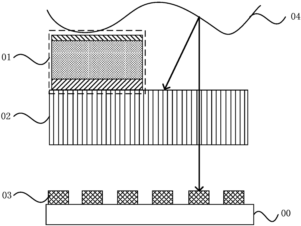
[0035] figure 1 It is a structural schematic diagram of an existing array substrate. refer to figure 1 , the array substrate includes a base substrate 00 , a light emitting unit 01 , a light screening structure 02 and a photosensitive unit 03 . The light emitting unit 01 is located on the base substrate 00 . The photosensitive unit 03 is located between the light emitting unit 01 and the base substrate 00 . The light screening structure 02 is located between the light emitting unit 01 and the photosensitive un...


PUM


Abstract

The embodiment of the invention discloses an array substrate, a manufacturing method of the array substrate, a display panel and a display device. The array substrate comprises a substrate body, a plurality of light emitting units located on the substrate body and light sensing units arranged on the sides, close to the substrate body, of the light emitting units; each light emitting unit comprisesa first electrode and a light emitting layer, and the first electrodes are located between the substrate body and the light emitting layers; each first electrode comprises at least one hollowed-out area and a non-hollowed-out area surrounding the hollowed-out area; vertical projections of the light sensing units on the substrate body are at least partially overlapped with the vertical projectionsof the hollowed-out areas of the first electrodes on the substrate body. Compared with an existing array substrate, the array substrate can achieve the aim of improving the fingerprint identificationprecision of the array substrate or even the display panel.

Description

technical field [0001] The present invention relates to display technology, in particular to an array substrate, a manufacturing method of the array substrate, a display panel and a display device. Background technique [0002] Each person's skin texture varies in pattern, breakpoints and intersections, and is unique to an individual and remains the same throughout life. Accordingly, the true identity of each person can be verified through skin texture recognition technology. At the same time, the fingerprint formed on the surface of the end of an individual's finger is easy to obtain because of its texture characteristics, and the individual can usually be associated with its fingerprint. By comparing the acquired fingerprint with the pre-saved fingerprint data, the true identity of the individual can be verified. This is fingerprint identification technology. In recent years, thanks to the combination and development of electronic integrated manufacturing technology and ...

Claims


Application Information

Patent Timeline
Patent Type & Authority Applications(China)
IPC IPC(8): H01L27/32
CPCH10K59/00H10K59/12
Inventor 程爽牛晶华王湘成朱晴那晓曦文磊张治
Owner WUHAN TIANMA MICRO ELECTRONICS CO LTD
Why Eureka
Try Eureka