Pixel circuit, array substrate, display panel and electronic equipment
A technology of pixel circuits and input terminals, which is applied in the fields of pixel circuits, display panels, electronic equipment, and array substrates, can solve problems such as the inability to meet the requirements of high image quality, and achieve the effect of meeting the requirements of high image quality.
- Summary
- Abstract
- Description
- Claims
- Application Information
AI Technical Summary
Problems solved by technology
Method used
Image

Examples
Embodiment 1
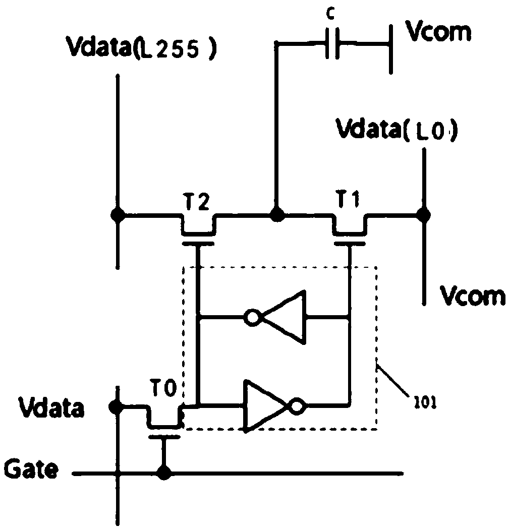
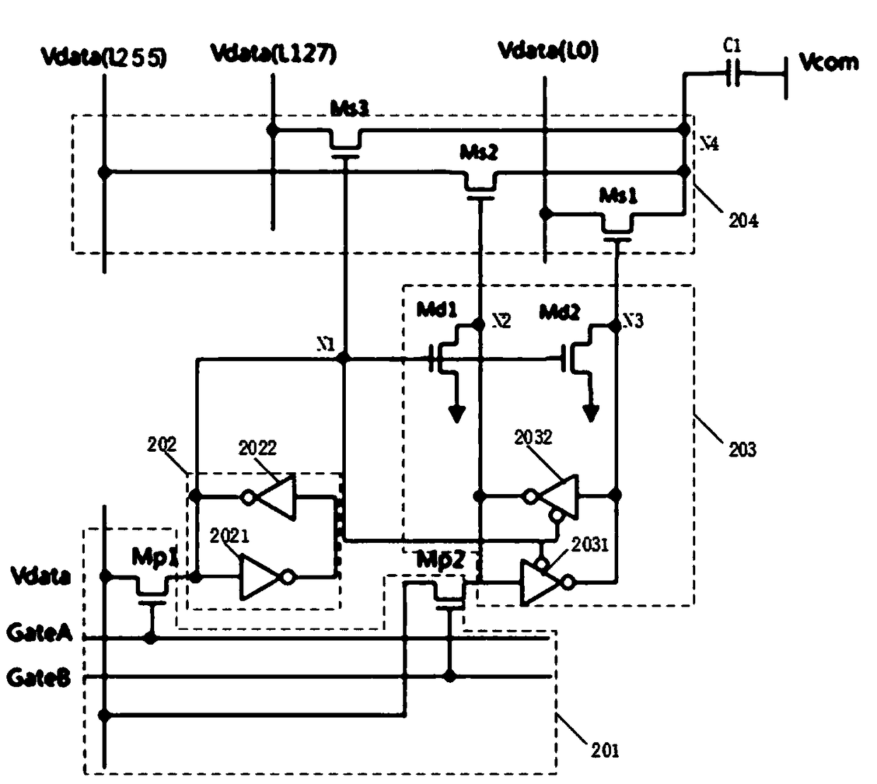
[0041] figure 2 A schematic diagram of a pixel circuit provided in the embodiment of the present application, such as figure 2 As shown, the pixel circuit includes: a data writing unit 201, a first data storage unit 202, a second data storage unit 203 and a light emission control unit 204;
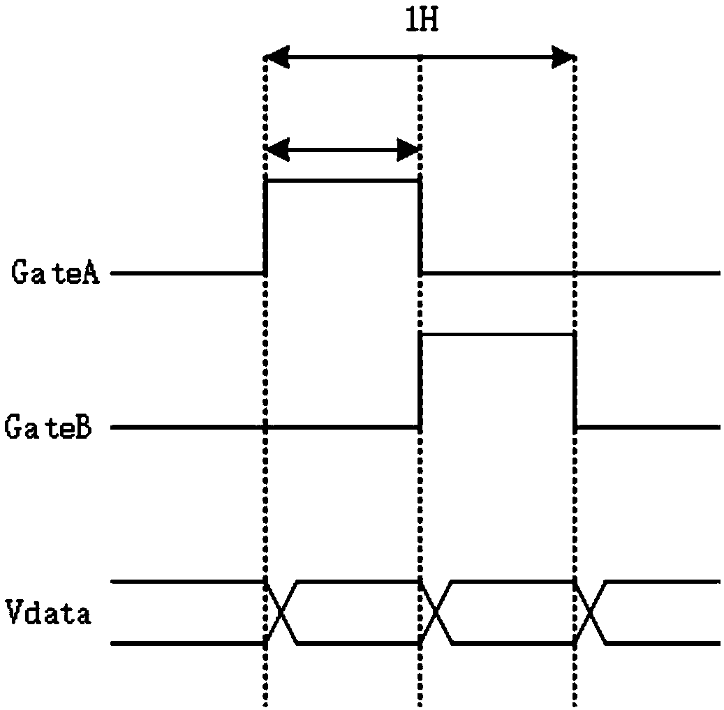
[0042] The data writing unit 201 is connected with the data signal input terminal Vdata, the first control signal input terminal GateA, the second control signal input terminal GateB, the first data storage unit 202 and the second data storage unit 203; Under the control of the input signal of the input terminal GateA, write the data signal of the data signal input terminal Vdata into the first data storage unit 202, and under the control of the input signal of the second control signal input terminal GateB, write the data of the data signal input terminal Vdata Write the signal into the second data storage unit 203;
[0043] The first data storage unit 202 is connected to the data wri...
Embodiment 2
[0054] Based on the pixel circuit structure provided in Embodiment 1 of the present application, Embodiment 2 of the present application specifically introduces the specific structure of each unit in the pixel circuit.
[0055] Optionally, the data writing unit 201 includes: a first thin film transistor Mp1 and a second thin film transistor Mp2;
[0056] The gate of the first thin film transistor Mp1 is connected to the first control signal input terminal GateA, the first pole (such as the source) of the first thin film transistor Mp1 is connected to the data signal input terminal Vdata, and the second pole of the first thin film transistor Mp1 ( Such as the drain) is connected to the first data storage unit 202;
[0057] The gate of the second thin film transistor Mp2 is connected to the second control signal input terminal GateB, the first pole (such as the source) of the second thin film transistor Mp2 is connected to the data signal input terminal Vdata, and the second pol...
Embodiment 3
[0094] Based on the same idea, an embodiment of the present application provides an array substrate, the array substrate includes: a plurality of data lines and a plurality of gate lines, and a plurality of sub-pixels defined by the insulating intersections of the plurality of data lines and the plurality of gate lines Each sub-pixel unit is provided with a pixel circuit as provided in the first aspect of the embodiment of the present application; each row of sub-pixel units corresponds to two gate lines, one of which is connected to the first control signal input terminal, and the other One gate line is connected to the second control signal input end; each row of sub-pixel units corresponds to a data line, and the data line is connected to the data signal input end.
[0095] Since the array substrate provided by the embodiment of the present application includes a plurality of sub-pixel units, and each sub-pixel unit is provided with the pixel circuit provided in the first as...
PUM
 Abstract
Description
Claims
Application Information
 - R&D
- Intellectual Property
- Life Sciences
- Materials
- Tech Scout
- Unparalleled Data Quality
- Higher Quality Content
- 60% Fewer Hallucinations
Browse by: Latest US Patents, China's latest patents, Technical Efficacy Thesaurus, Application Domain, Technology Topic, Popular Technical Reports.
© 2025 PatSnap. All rights reserved.Legal|Privacy policy|Modern Slavery Act Transparency Statement|Sitemap|About US| Contact US: help@patsnap.com