OLED display panel and pixel arrangement structure thereof

A pixel arrangement and pixel technology, which is applied to electrical components, electrical solid devices, circuits, etc., can solve the problems of increasing the difficulty of G sub-pixels, and achieve the effects of reducing production difficulty, small space area, and excellent image quality

Active Publication Date: 2018-12-07
WUHAN CHINA STAR OPTOELECTRONICS SEMICON DISPLAY TECH CO LTD
View PDF6 Cites 11 Cited by
  • Summary
  • Abstract
  • Description
  • Claims
  • Application Information

AI Technical Summary

Problems solved by technology

Due to the characteristics of the light-emitting materials of the R, G, and B sub-pixels, the attenuation speed of the B sub-pixel is faster than the other two. The area should be the largest, and the area of ​​the G sub-pixel is the smallest, which increases the difficulty of making the G sub-pixel

Method used


Image

  • OLED display panel and pixel arrangement structure thereof
  • OLED display panel and pixel arrangement structure thereof
  • OLED display panel and pixel arrangement structure thereof

Examples


Embodiment Construction

[0029] The following descriptions of various embodiments refer to the accompanying drawings to illustrate specific embodiments in which the present invention can be implemented.

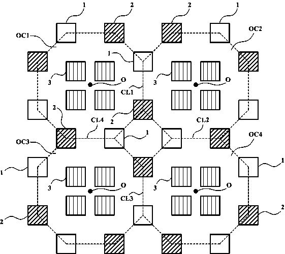
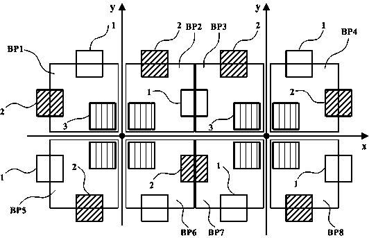
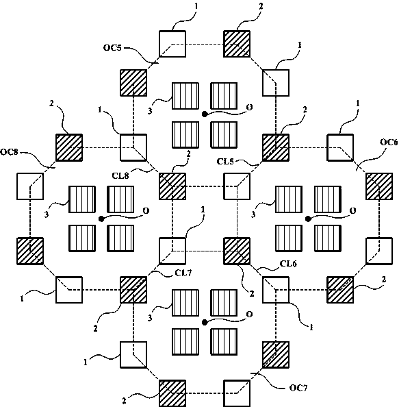
[0030] Please refer to figure 1 As shown, Embodiment 1 of the present invention provides a pixel arrangement structure, including:

[0031] A plurality of first sub-pixels 1, a plurality of second sub-pixels 2 and a plurality of third sub-pixels 3, the plurality of first sub-pixels 1, a plurality of second sub-pixels 2 and a plurality of third sub-pixels 3 form multiple repeated virtual octagons;

[0032] The third sub-pixel 3 is arranged inside the virtual octagon, and four third sub-pixels 3 are arranged inside each virtual octagon, and the four third sub-pixels 3 are arranged in the virtual octagon. The center of the octagon is symmetrically arranged;

[0033] The first sub-pixel 1 is spaced apart from the third sub-pixel 3 and has a center at a first vertex of the virtual octagon;

[0034] Th...


PUM


Abstract

The present invention provides an OLED display panel and a pixel arrangement structure thereof. The pixel arrangement structure comprises a plurality of repeatedly arranged virtual n polygons formed by a plurality of first sub pixels, a plurality of second sub pixels and a plurality of third sub pixels, where n is an even number being larger than or equal to 4, the third sub pixels are arranged inthe virtual n polygons, each virtual n polygon is internally provided with n / 2 third sub pixels, the first sub pixels and the third sub pixels are separated from each other and have centers at the first vertexes of the n polygons; and the second sub pixels are separated from the first sub pixels and the third sub pixels and has the center of the second vertexes of a virtual octagon. The OLED display panel and the pixel arrangement structure thereof can reduce the quantity of the sub pixels and can reduce the occupation area of each basic element unit; and the third sub pixels are located at the center of the n polygons and can commonly use one FMM opening so as to reduce the evaporation difficulty.

Description

technical field [0001] The invention relates to the technical field of screen display, in particular to an OLED display panel and a pixel arrangement structure thereof. Background technique [0002] Organic light-emitting diode OLED (Organic light-emitting Diode) self-luminous display through the organic layer, because it does not require a backlight source, it has faster response time, larger viewing angle, higher contrast ratio and lighter component quality , low power consumption and other characteristics, it is currently recognized as the most potential flat panel display technology. [0003] In order to achieve a higher resolution of the OLED panel, at the current level of process technology, it can only be realized by sub-pixel rendering. The sub-pixel rendering technology mainly realizes normal display by borrowing the R, G, and B sub-pixels of adjacent pixels. Due to the characteristics of the light-emitting materials of the R, G, and B sub-pixels, the attenuation ...

Claims


Application Information

Patent Timeline
Patent Type & Authority Applications(China)
IPC IPC(8): H01L27/32
CPCH10K59/353
Inventor 李豪凯
Owner WUHAN CHINA STAR OPTOELECTRONICS SEMICON DISPLAY TECH CO LTD
Why Eureka
Try Eureka