Multilayer stacked 3D-SIP chip test method

A technology of chip testing and multi-layer stacking, which is applied in the direction of electronic circuit testing, measuring electricity, measuring devices, etc., can solve the problems of increasing difficulty in the testing stage, and achieve the effect of saving a large number of pins and flexible application

Active Publication Date: 2019-04-09
WUXI ZHONGWEI TENGXIN ELECTRONICS
View PDF6 Cites 10 Cited by
  • Summary
  • Abstract
  • Description
  • Claims
  • Application Information

AI Technical Summary

Problems solved by technology

However, this also makes the testing phase more difficult
[0003] During the wafer stacking process, with the increase in the number of stacked wafers and the introduction of new defects in the manufacturing process, new testing challenges are brought

Method used


Image

  • Multilayer stacked 3D-SIP chip test method
  • Multilayer stacked 3D-SIP chip test method
  • Multilayer stacked 3D-SIP chip test method

Examples


Embodiment Construction

[0025] Specific embodiments of the present invention will be described in detail below in conjunction with the accompanying drawings. It should be understood that the specific embodiments described here are only used to illustrate and explain the present invention, and are not intended to limit the present invention.

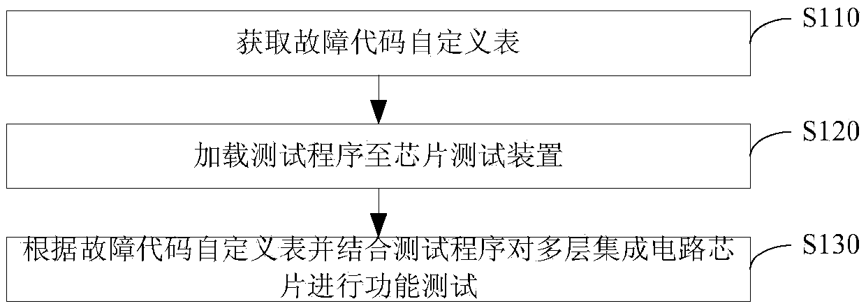
[0026] As an aspect of the present invention, a kind of 3D-SIP chip testing method of multi-layer stacking is provided, wherein, as figure 1 Shown, described 3D-SIP chip test method comprises:

[0027] S110. Acquiring a custom fault code table;

[0028] S120, load the test program to the chip test device;

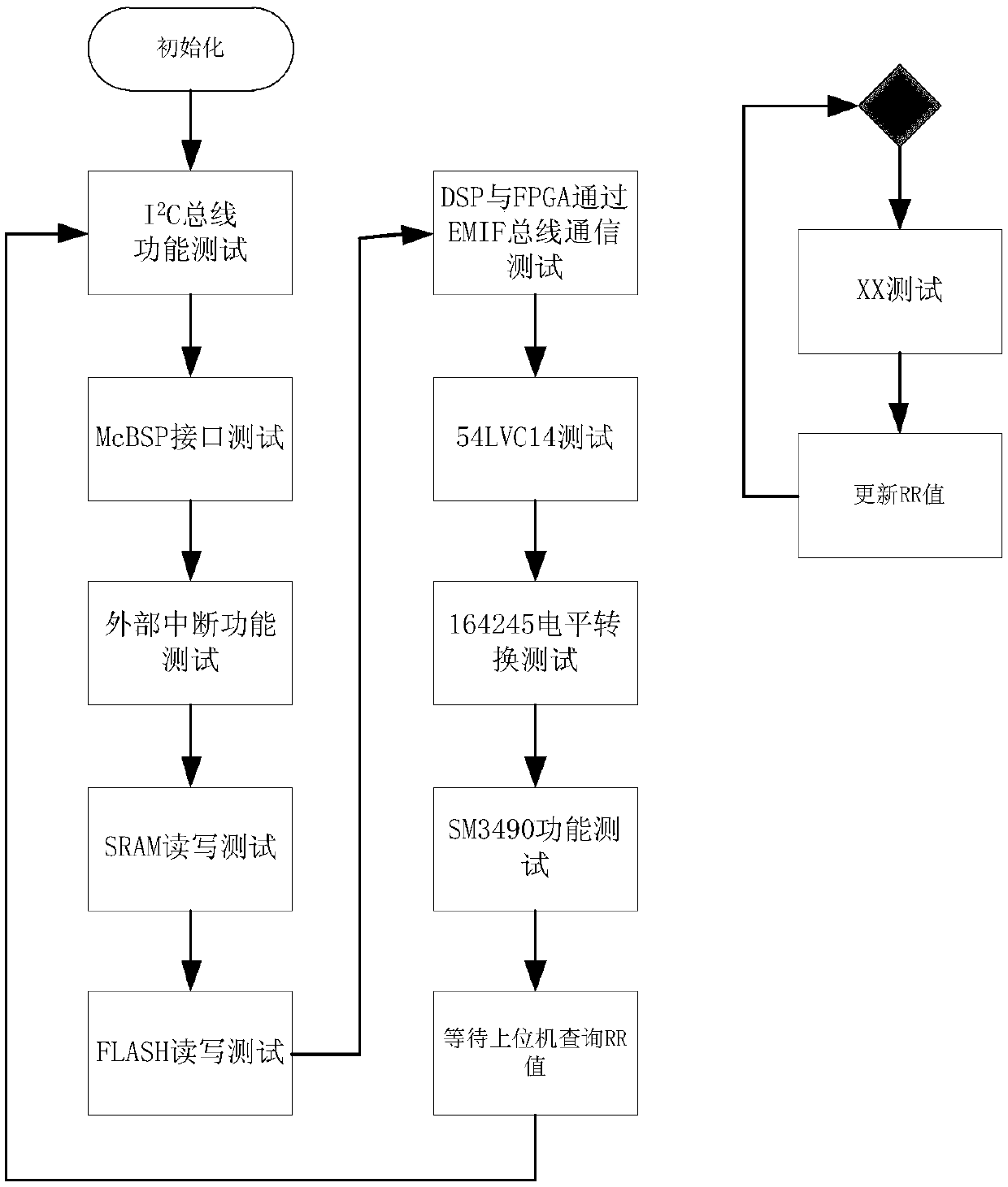
[0029] S130. Perform a functional test on the multilayer integrated circuit chip according to the fault code custom table and in combination with the test program;

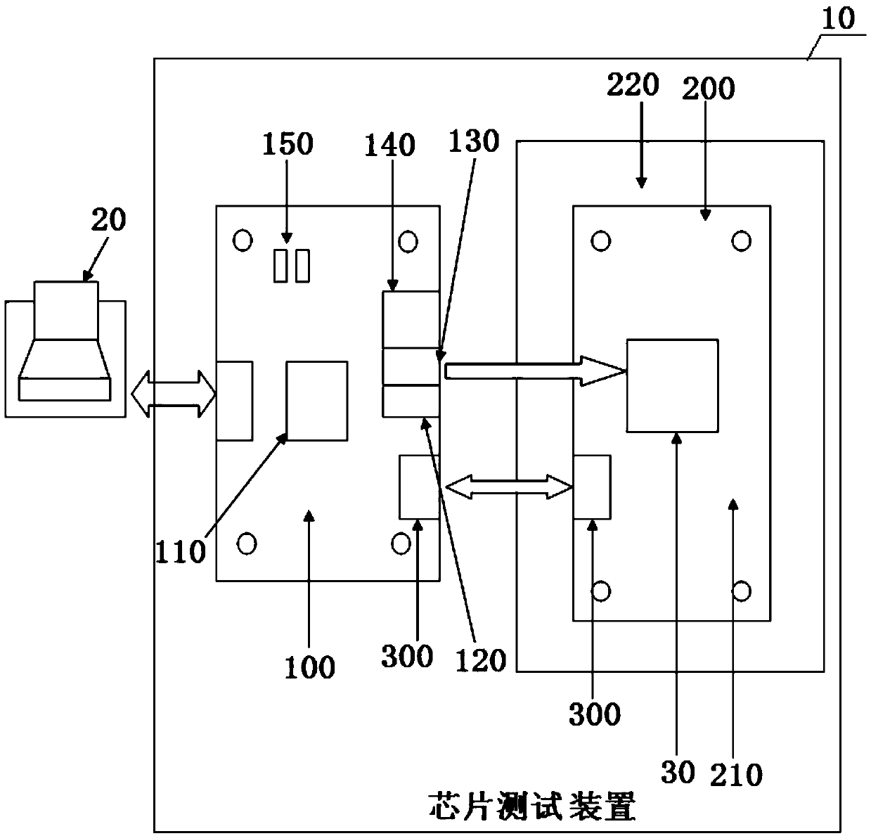
[0030] Wherein, the chip testing device is used for executing a test program and for installing the multi-layer integrated circuit chip.

[0031] The multi-layer stacked 3D-SIP chip testing m...


PUM


Abstract

The invention relates to the technical field of integrated circuit test, and specifically discloses a multilayer stacked 3D-SIP chip test method. The 3D-SIP chip test method comprises the steps of: obtaining a fault code user-defined table; loading a test program to a chip test device; and carrying out function test on a multilayer integrated circuit chip according to the fault code user-defined table and the test program, wherein the chip test device is used for executing the test program and installing the multilayer integrated circuit chip. The multilayer stacked 3D-SIP chip test method iscapable of carrying out automatic function test on multilayer integrated circuit chips, saving the troubles of large pin number and complicated development program, carrying out multiple tests via flexible application, and realizing 100% function test.

Description

technical field [0001] The invention relates to the technical field of integrated circuit testing, in particular to a multilayer stacked 3D-SIP chip testing method. Background technique [0002] Wafer-level chips are heterogeneously integrated with a large number of cores, resulting in increased test complexity and cost. When designing 3D-SiP chips, some circuits may be divided into different wafer layers to minimize the interconnection length, which greatly improves the performance of 3D-SiP. However, this also makes the testing phase more difficult. [0003] During the wafer stacking process, with the increase in the number of stacked wafers and the introduction of new defects in the manufacturing process, new testing challenges are brought. Therefore, how to provide a test method suitable for multi-chip stacking has become a technical problem to be solved urgently by those skilled in the art. Contents of the invention [0004] The present invention aims to solve at l...

Claims


Application Information

Patent Timeline
Patent Type & Authority Applications(China)
IPC IPC(8): G01R31/28
CPCG01R31/2851
Inventor 张凯虹徐德生奚留华武乾文
Owner WUXI ZHONGWEI TENGXIN ELECTRONICS
Why Eureka
Try Eureka