Optical fiber
An optical fiber and fiber core technology, which can be used in polarized fibers, clad fibers, optics, etc., and can solve problems such as increased SSC loss.
Active Publication Date: 2019-04-16
FUJIKURA LTD
View PDF8 Cites 0 Cited by
- Summary
- Abstract
- Description
- Claims
- Application Information
AI Technical Summary
Problems solved by technology
However, if the mode field diameter of the semiconductor optical waveguide is enlarged to the s
Method used
View moreImage
Smart ImageViewing Examples
Examples
 PUM
| Property | Measurement | Unit |
|---|---|---|
| Mode field diameter | aaaaa | aaaaa |
Abstract
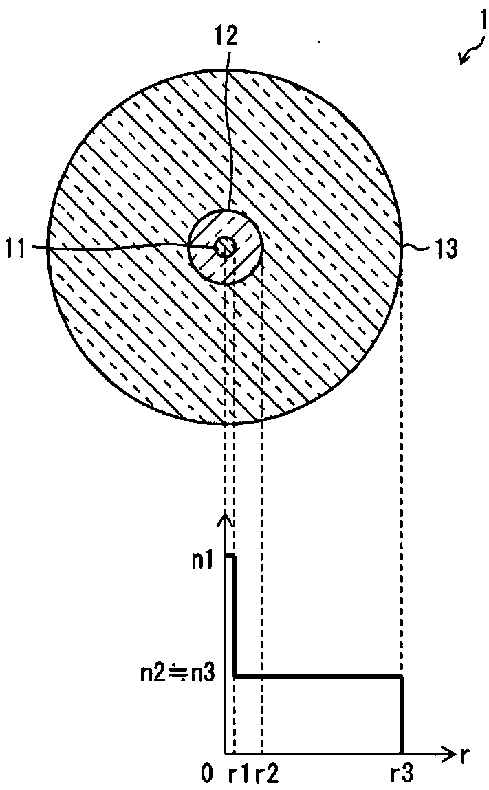
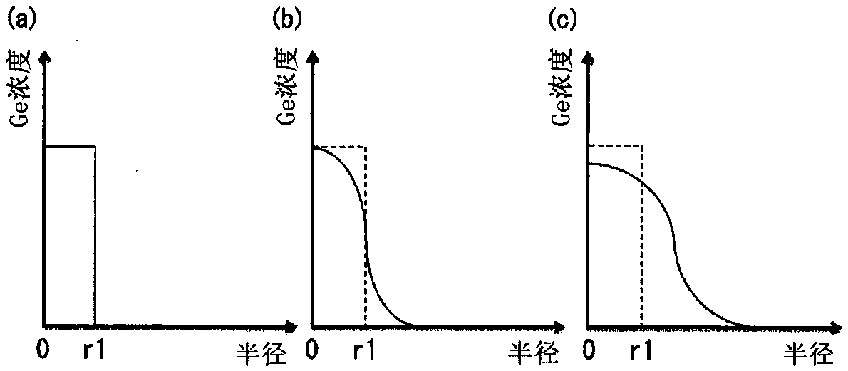
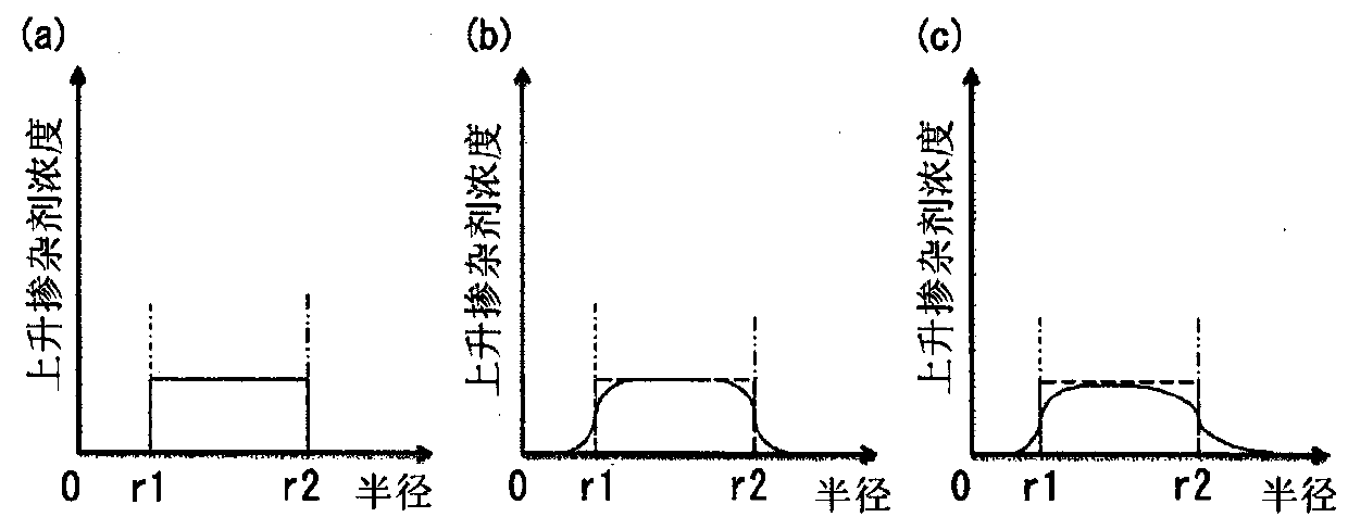
Provided is an optical fiber capable of sufficiently reducing the connection loss at a fusion splice point with a CSMF. The optical fiber is configured such that the refractive index of inner cladding(12) is substantially the same as the refractive index of outer cladding (13) while the concentration of the up-dopant in the inner cladding (12) is set so that the rate of increase of the refractiveindex due to the up-dopant is between 0.25% and 0.5%, inclusive.
Description
technical field [0001] The present invention relates to an optical fiber capable of expanding the core by thermal diffusion. Background technique [0002] Semiconductor optical waveguides typified by silicon optical waveguides are highly expected as technologies that contribute to the integration of optical communication devices. For example, silicon waveguides with functions such as optical modulators, optical detectors, and optical switches have been realized, and the utilization of optical communication has begun. [0003] In order to propagate light input to or output from the semiconductor optical waveguide, the semiconductor optical waveguide is often connected to a CSMF (Conventional Single Mode Fiber: Conventional Single Mode Fiber). However, while the mode field diameter of a semiconductor optical waveguide is about 1 μm, the mode field diameter of CSMF is about 10 μm. Therefore, if the CSMF is butt-connected to the semiconductor optical waveguide, the connection ...
Claims
Login to View More Application Information
Patent Timeline
 IPC IPC(8): G02B6/036G02B6/024G02B6/30
CPCG02B6/024G02B6/036G02B6/30G02B6/03694G02B6/03622G02B6/02004G02B6/2551G02B6/305G02B6/0286C03C3/06C03C2201/12C03C2201/31C03C13/045C03C2201/28C03C2201/10G02B6/255
Inventor 平川圭祐市井健太郎林和幸
Owner FUJIKURA LTD


