Display panel
A display panel and display area technology, applied in the direction of organic semiconductor devices, instruments, electrical components, etc., can solve problems such as poor flexibility, broken metal wiring, broken insulating layer, etc., and achieve the effect of reducing the risk of fracture and preventing the longitudinal extension of cracks
- Summary
- Abstract
- Description
- Claims
- Application Information
AI Technical Summary
Problems solved by technology
Method used
Image
Examples
Embodiment Construction
[0024] The specific implementation manners of the display panel provided by the present invention will be described in detail below in conjunction with the accompanying drawings.
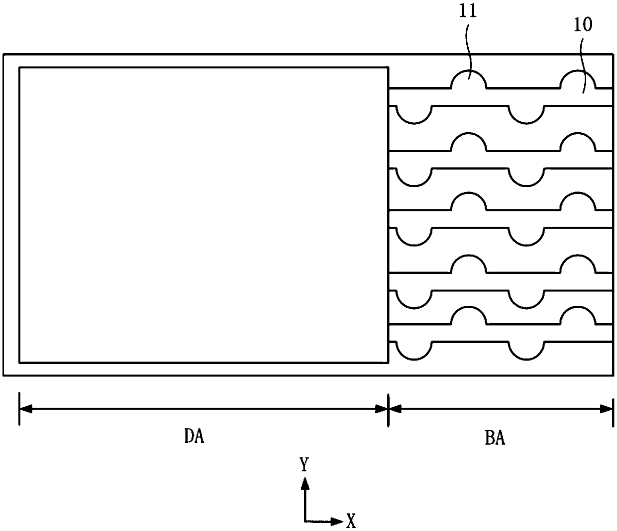
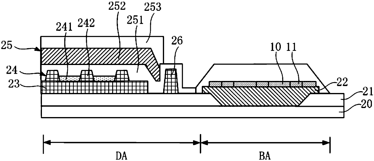
[0025] figure 1 It is a top view structure diagram of the first embodiment of the display panel of the present invention, figure 2 It is a schematic diagram of the side structure of the first embodiment of the display panel of the present invention. see figure 1 and figure 2 , the display panel of the present invention includes a display area DA and a bending area BA.
[0026] The display area DA refers to an area serving as a display surface of a display panel. The bending area BA refers to an area that can be bent, wherein the bending area BA can be bent relative to the display area DA. Specifically, the bending area BA can be bent toward the back of the display area DA. The back side of the display area DA refers to the side of the display panel that does not need to be displayed. In thi...
PUM
 Abstract
Description
Claims
Application Information


