Semiconductor device and manufacturing method thereof

A manufacturing method and semiconductor technology, applied in the fields of semiconductor/solid-state device manufacturing, semiconductor devices, electrical components, etc., can solve the problems of inability to meet the performance of MOSFET devices, easy to generate leakage current, short-channel effect, etc., to improve the reverse short-channel Channel effect, reduce junction capacitance, reduce the effect of junction leakage

Active Publication Date: 2019-05-14
SEMICON MFG INT (SHANGHAI) CORP +1
View PDF5 Cites 1 Cited by
  • Summary
  • Abstract
  • Description
  • Claims
  • Application Information

AI Technical Summary

Problems solved by technology

However, it has been found in practice that MOSFET devices with embedded silicon germanium / silicon carbon source-drain structures formed in the prior art are still prone to leakage currents or short channel effects, which still cannot meet the requirements for further improvement in the performance of MOSFET devices

Method used


Image

  • Semiconductor device and manufacturing method thereof
  • Semiconductor device and manufacturing method thereof
  • Semiconductor device and manufacturing method thereof

Examples


Embodiment Construction

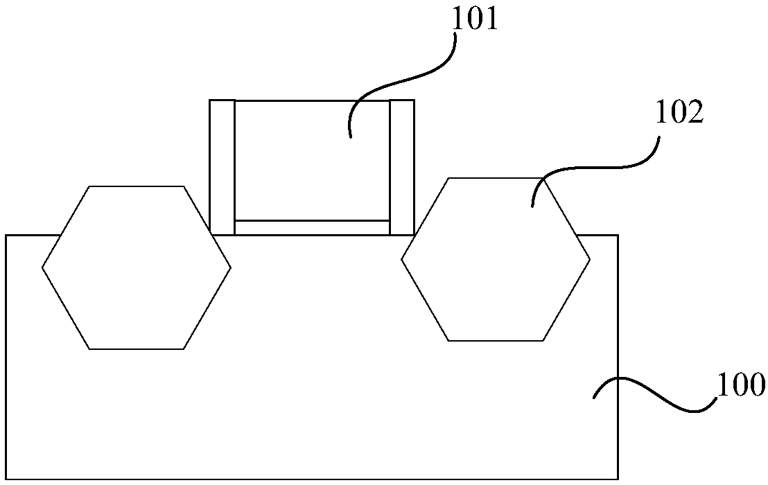
[0049] Please refer to figure 1 , a PMOS transistor comprising a semiconductor substrate 100, a gate stack structure 101 formed on the surface of the semiconductor substrate 100, and an embedded silicon germanium source and drain formed in the semiconductor substrate 100 on both sides of the gate stack structure 101 102, the formation process includes etching the semiconductor substrate 100 on both sides of the gate stack structure 101 to form a "Σ (Sigma)" shaped source-drain groove; The silicon germanium stress layer is epitaxially grown in the groove, or a stress seed layer is first grown, and then the silicon germanium stress layer is epitaxially grown to form the embedded silicon germanium source and drain 102 .

[0050] With the shrinking of the gate length of transistors, such as entering the 28nm technology node, the short channel effect (SCE) and short channel effect (RSCE) become the key restrictive factors for the performance improvement of the above-mentioned PMOS ...


PUM


Abstract

The invention provides a semiconductor device and a manufacturing method thereof. Ion injection is at least performed on a surface of a first stress seed layer after the first stress seed layer is formed in a source-drain groove, a second stress seed layer is formed on the first stress seed layer, a relatively smooth contact interface can be provided for the second stress seed layer by the first stress seed layer, the epitaxial growth rate of the second stress seed layer at each position on a surface of the first stress seed layer can be controlled by injected ions in the first stress seed layer, so that the finally-formed target shape of the second stress seed layer can be controlled, a shallower junction can be generated at a channel edge below a gate stack structure, higher channel control is generated, the junction capacitance and junction electricity leakage are reduced, a short-channel effect and an inverse short-channel effect are improved, and the performance improvement requirement of the device is met.

Description

technical field [0001] The invention relates to the technical field of integrated circuit manufacturing, in particular to a semiconductor device and a manufacturing method thereof. Background technique [0002] After MOSFET devices are scaled down to 45nm, high-K metal gate (HKMG) needs to be used to suppress the defects of higher gate leakage and reduced gate capacitance due to the problem of polysilicon gate depletion. Epitaxial growth of silicon germanium or silicon carbon in the source and drain grooves (PSR / NSR) formed by etching the source and drain regions to form an embedded silicon germanium / silicon carbon source and drain structure (ie e-SiGe / e-SiC) to provide The compressive stress squeezes the channel or provides the tensile stress to stretch the channel, suppress the short channel effect (SCE), improve the carrier mobility, and thus improve the performance of the MOSFET. However, it has been found in practice that MOSFET devices with embedded silicon germanium / ...

Claims


Application Information

Patent Timeline
Patent Type & Authority Applications(China)
IPC IPC(8): H01L29/08H01L29/423H01L29/78H01L21/336H01L21/28
Inventor 赵猛
Owner SEMICON MFG INT (SHANGHAI) CORP
Why Eureka
Try Eureka