Structure and manufacturing method of a micro-led display

A technology for display screens and display arrays, which is used in semiconductor/solid-state device manufacturing, identification devices, and semiconductor/solid-state device components, etc., which can solve the problem that metal leads cannot be fabricated, the proportion of the effective display area of ​​the display screen is reduced, and the non-display area is occupied. area, etc.

Active Publication Date: 2020-07-07
福州市福大微纳显示科技有限公司
View PDF6 Cites 1 Cited by
  • Summary
  • Abstract
  • Description
  • Claims
  • Application Information

AI Technical Summary

Problems solved by technology

In traditional large-size LED displays, these common-cathode and common-anode metal leads can be fabricated directly on the PCB, but in Micro-LED displays, extremely small-width metal leads cannot be fabricated on the PCB
In order to solve this problem, metal leads can be made directly on the display screen, but this will occupy a certain area of ​​the non-display area. In addition, it will also occupy a certain area when the driver chip is thermally pressed on the display screen. It will reduce the effective display area ratio of the display

Method used


Image

  • Structure and manufacturing method of a micro-led display
  • Structure and manufacturing method of a micro-led display
  • Structure and manufacturing method of a micro-led display

Examples


Embodiment Construction

[0033] In order to make the above-mentioned features and advantages of the present invention more comprehensible, the following specific embodiments are described in detail with reference to the accompanying drawings, but the present invention is not limited thereto.

[0034] refer to Figure 1 to Figure 6

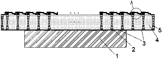
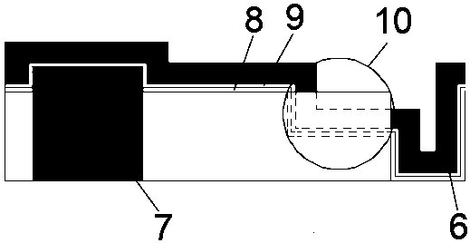
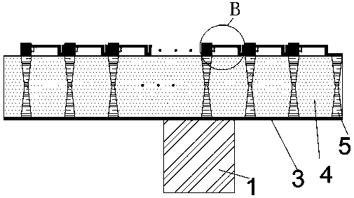
[0035] A Micro-LED display structure, including a display array arranged on the front of the display (the front of the glass substrate) and composed of Micro-LED chips, the Micro-LED chips in each row and column in the display array are respectively connected by metal wires , and a layer of insulating layer is provided between the surface of the display array and the metal lines of rows and columns; the back of the display screen is provided with a driver chip 1, a metal pad 2 and several back metal wires with one end connected to the driver chip. Routing 3, each metal wire on the back is in one-to-one correspondence with the metal wires on the front; the metal wires on t...


PUM


Abstract

The invention relates to a Micro-LED display screen structure and a production method and relates to the technical field of displayers. The Micro-LED display screen structure comprises a display arraywhich is arranged on the front of a display screen and composed of Micro-LED chips, wherein the Micro-LED chips in each row and the Micro-LED chips in each column of the display array are connected through metal wires respectively, an insulation layer is arranged between the surface of the display array and the metal wire in each row, and an insulation layer is arranged between the surface of thedisplay array and the metal wire in each column; a driving chip, a metal bonding pad and a plurality of back metal wires are arranged on the back of the display screen, wherein one end of each back metal wire is connected with the driving chip, and all the back metal wires are functionally in one-to-one correspondence with the front metal wires; and the front metal wires of the display screen andthe back metal wires in one-to-one correspondence with the front metal wires are connected through holes and form channels. Through the Micro-LED display screen structure and the production method, problems concerning transfer and bonding in the design and production process of the Micro-LED display screen are effectively overcome.

Description

technical field [0001] The invention relates to a structure and a manufacturing method of a Micro-LED display screen, and relates to the technical field of displays. Background technique [0002] Micro-LED refers to the miniaturization of the traditional LED structure. Because the brightness, life, contrast, response time, power consumption, viewing angle and other performances of Micro-LED technology are superior to LCD and OLED technology, plus It is self-illuminating, simple in structure, and highly adaptable to the environment. It has been regarded as the next-generation display technology by many manufacturers and has begun to actively deploy it. [0003] At present, the structure of the Micro-LED display is mainly the combination of the Micro-LED chip and the CMOS or TFT driver backplane, and the Micro-LED chip is integrated on the CMOS or TFT driver backplane by means of transfer and bonding to form a Complete display structure. However, the transfer technology of M...

Claims


Application Information

Patent Timeline
Patent Type & Authority Patents(China)
IPC IPC(8): H01L23/498H01L33/62H01L27/15H01L21/48H01L21/603G09F9/33
CPCH01L2224/18
Inventor 林志贤郑泽平叶芸严群郭太良张永爱周雄图
Owner 福州市福大微纳显示科技有限公司
Why Eureka
Try Eureka