Non-volatile ferroelectric memory device and method of driving same

A ferroelectric storage, non-volatile technology, used in static memory, electric solid state devices, digital memory information, etc., to improve the dispersion of threshold voltage, improve the working speed, and improve the refresh range.

Pending Publication Date: 2019-08-30
SAMSUNG ELECTRONICS CO LTD
View PDF8 Cites 6 Cited by
  • Summary
  • Abstract
  • Description
  • Claims
  • Application Information

AI Technical Summary

Problems solved by technology

This problem can be a big obstacle for realizing non-volatile NAND memory devices using ferroelectric field effect transistors

Method used


Image

  • Non-volatile ferroelectric memory device and method of driving same
  • Non-volatile ferroelectric memory device and method of driving same
  • Non-volatile ferroelectric memory device and method of driving same

Examples


Embodiment Construction

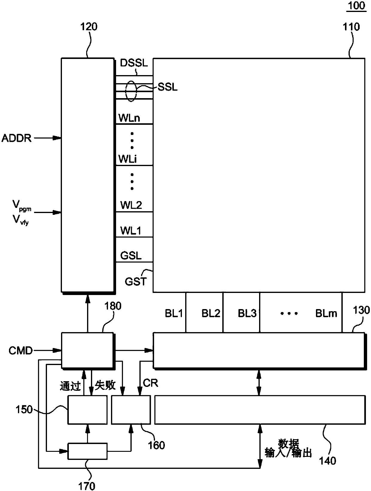
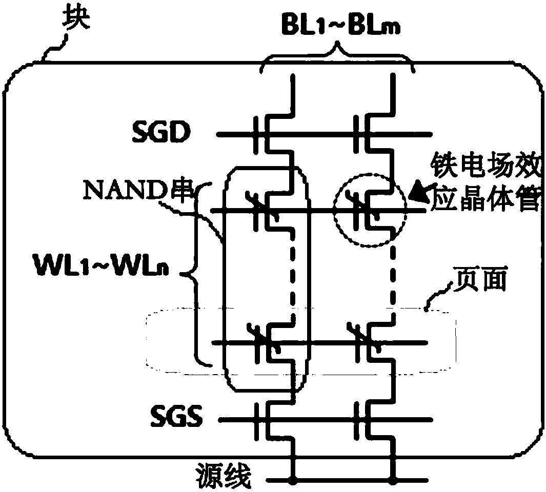
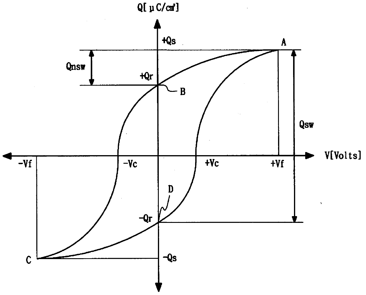
[0027] Hereinafter, preferred embodiments of the present invention will be described in detail with reference to the accompanying drawings.

[0028] The multiple embodiments of the present invention are used to make those of ordinary skill in the art of the present invention understand the present invention more completely. The following embodiments can be modified in various ways, and the scope of the present invention is not limited to the following embodiments. Rather, these embodiments make this disclosure more substantial and complete, and are used to fully convey the idea of ​​the present invention to those skilled in the art to which the present invention belongs.

[0029] In the figures, the same reference numerals refer to the same elements. And, as used in this specification, the term "and / or" includes one of the listed items and all combinations of more than one.

[0030] The terms used in this specification are for describing the embodiments, and do not limit the ...


PUM


Abstract

The invention relates to a non-volatile ferroelectric memory device and a method of driving the same. The present invention relates to a non-volatile ferroelectric memory device including a semiconductor active layer, a plurality of memory cells connected in series on the semiconductor active layer, and a control circuit for performing a read operation and a program operation on the selected memory cell among the plurality of memory cells, each of the memory cells comprising a para-dielectric layer on the semiconductor active layer; a dielectric stack including a ferroelectric layer stacked onthe para-dielectric layer and a charge trap site for generating a negative capacitance effect of the ferroelectric layer by charges disposed and trapped at an interface between the ferroelectric layer and the para-dielectric layer; and a control gate electrode on the ferroelectric layer.

Description

technical field [0001] The present invention relates to semiconductor technology, and more specifically, to a non-volatile ferroelectric memory device (Non-volatile ferroelectric memory device) and a driving method thereof. Background technique [0002] Recently, with the increasing demand for portable digital application devices such as digital cameras, MP3 players, PDAs (personal digital assistants) and mobile phones and the replacement of previous hard drives by solid-state drives (SSD, solid-state drives), non-volatile The memory market is expanding rapidly. A representative example of the aforementioned non-volatile memory device is a low-cost NAND flash memory device that can be highly integrated. [0003] The above-mentioned NAND flash memory devices have a transistor cell structure based on metal oxide semiconductor field effect transistors (MOSFETs), and are classified into floating gate type and charge trap type memory devices according to the type of information ...

Claims


Application Information

Patent Timeline
Patent Type & Authority Applications(China)
IPC IPC(8): G11C11/22
CPCG11C11/2273G11C11/2259G11C11/2255G11C11/2257G11C11/2275G11C11/221H10B51/30H01L29/78391H01L29/6684H01L29/516H01L29/40111H10B53/00
Inventor 黄哲盛
Owner SAMSUNG ELECTRONICS CO LTD
Why Eureka
Try Eureka