Touch substrate, preparation method and driving method thereof and touch display panel
A substrate and touch technology, which is applied in the fields of instruments, calculations, electrical digital data processing, etc., can solve the problems of difficult manufacturing process and high complexity of touch panel design
- Summary
- Abstract
- Description
- Claims
- Application Information
AI Technical Summary
Problems solved by technology
Method used
Image
Examples
no. 1 example
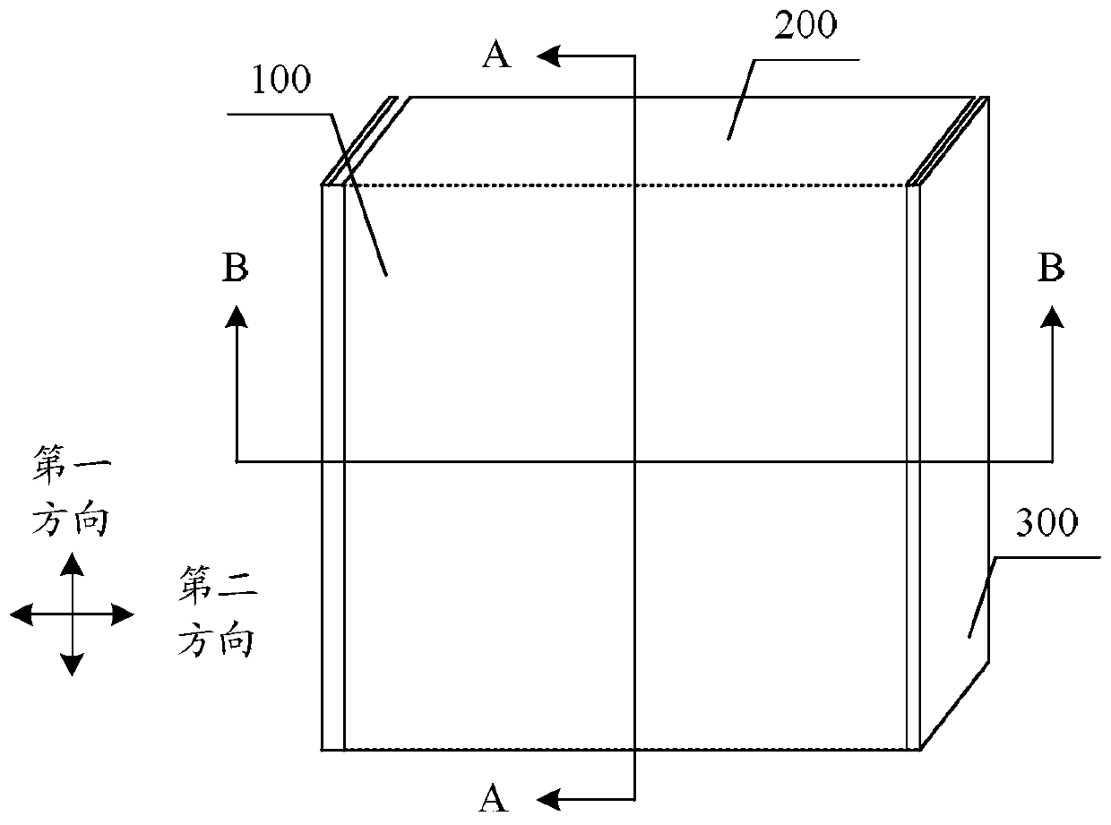
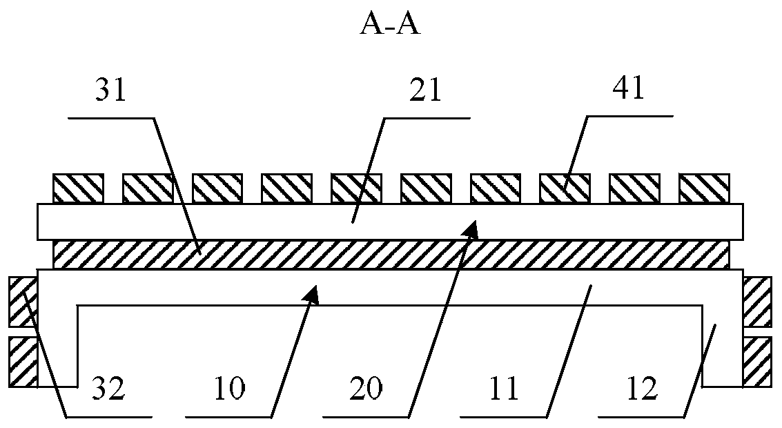
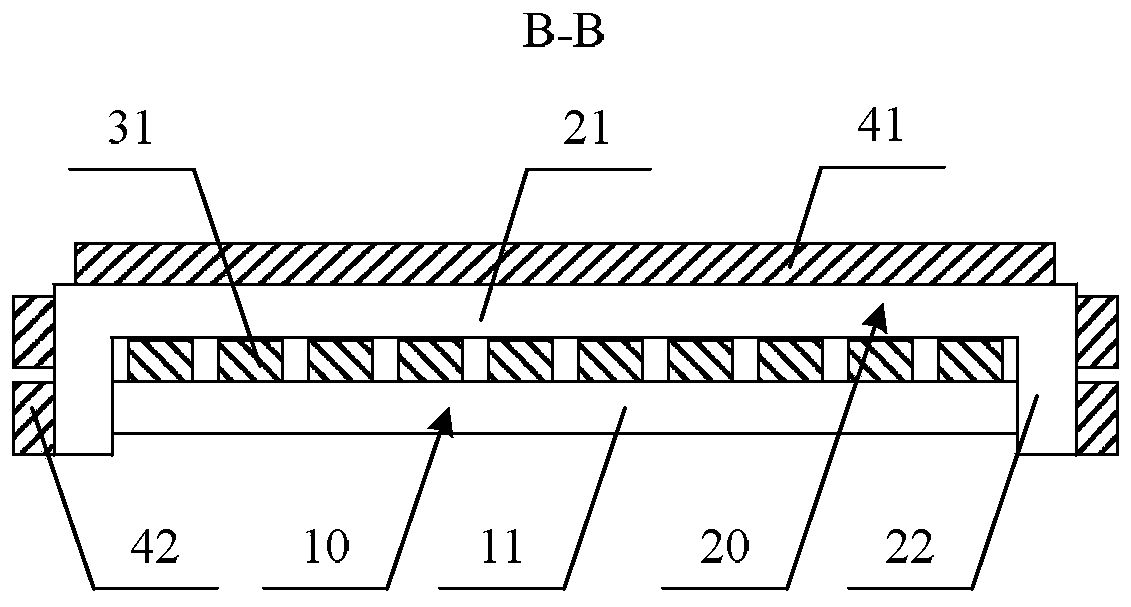
[0083] figure 1 It is a schematic structural diagram of the touch substrate according to the first embodiment of the present invention, figure 2 for figure 1 The sectional view of A-A in the middle, image 3 for figure 1 The cross-sectional view of B-B in the middle. Such as figure 1 As shown, on a plane parallel to the touch substrate, the main structure of the touch substrate in this embodiment includes a planar portion 100, two first bending portions 200 disposed opposite to each other in the first direction, and two oppositely disposed first bending portions 200 in the second direction. Two opposite second bending portions 300, the first bending portion 200 and the second bending portion 300 extend from the edge of the planar portion 100 and bend to the side of the planar portion 100, where the first bending portion 200 is The first edge is adjacent to the second edge where the second bending portion 300 is located, and the first direction and the second direction ar...
no. 2 example
[0097] Based on the technical idea of the aforementioned first embodiment, the embodiment of the present invention also provides a touch display panel. The touch display panel of this embodiment includes the touch substrate of the aforementioned first embodiment, and further includes a display panel and a cover plate, the touch substrate is disposed on the display panel, and the cover plate is disposed on the touch substrate.
[0098] In this embodiment, the touch display panel is an ON-Cell touch display panel. The preparation process of the touch display panel in this embodiment includes:
[0099] First, the display panel and the touch substrate are prepared respectively. Wherein, the prepared display panel includes a plane part and a bent part, and the bent part extends from the edge of the plane part and bends to the side of the plane part. The preparation process can adopt mature related technologies, the touch substrate and its preparation The process has been descri...
no. 3 example
[0104] Based on the technical idea of the aforementioned first embodiment, the embodiment of the present invention also provides a touch display panel. The touch display panel of this embodiment includes the touch substrate of the aforementioned first embodiment, and further includes a display panel and an encapsulation layer, the touch substrate is disposed in the display panel, and the encapsulation layer is disposed on the touch substrate.
[0105] In this embodiment, the touch display panel is an in-cell (IN-Cell) touch display panel. The preparation process of the touch display panel in this embodiment includes:
[0106] Firstly, the display structure layer 70 of the display panel is prepared. The prepared display structure layer 70 is in an unbent state, and the preparation process can adopt mature related technologies, which will not be repeated here.
[0107] Subsequently, a touch control substrate is prepared on the display structure layer 70 . Wherein, the struct...
PUM
 Abstract
Description
Claims
Application Information


