Laminating method of PCB and buffer layer

A kind of PCB circuit board, buffer layer technology, applied in the direction of printed circuit, multilayer circuit manufacturing, printed circuit manufacturing, etc., can solve the problems of cleaning and quality, kraft paper sticking to the bottom and cover of the steel plate and hot press, etc.

Inactive Publication Date: 2019-10-22
KALEX MULTI LAYER CIRCUIT BOARD (ZHONGSHAN) CO LTD
View PDF2 Cites 1 Cited by
  • Summary
  • Abstract
  • Description
  • Claims
  • Application Information

AI Technical Summary

Problems solved by technology

In terms of operating characteristics, after the kraft paper is pressed and heated, it is easy to cause the kraft paper to stick to the steel plate and the bottom and cover of the hot press, causing subsequent cleaning and quality problems.

Method used


Image

  • Laminating method of PCB and buffer layer
  • Laminating method of PCB and buffer layer
  • Laminating method of PCB and buffer layer

Examples


Embodiment 1

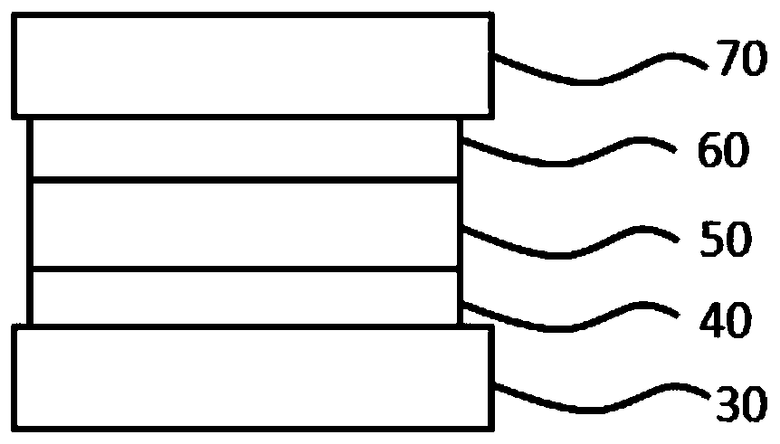
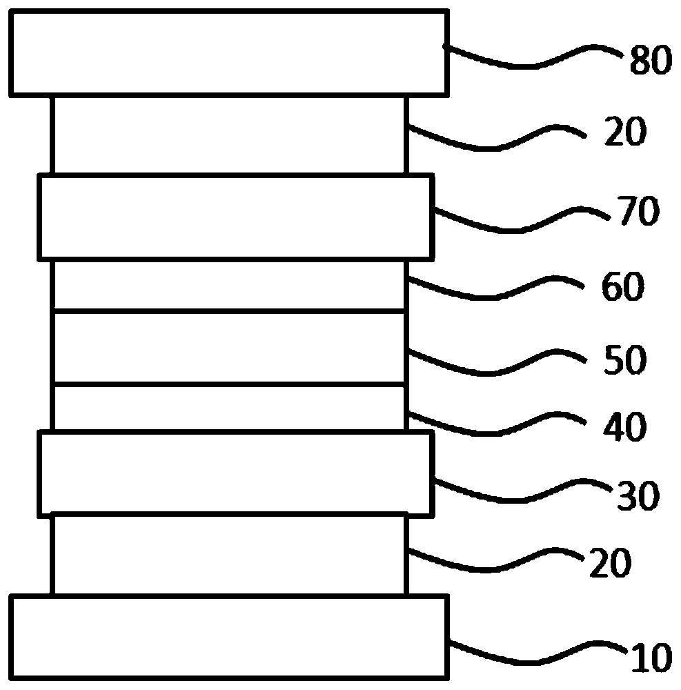
[0038] A method for pressing a PCB circuit board, comprising the following steps:

[0039] Browning: Oxidize the surface of the inner circuit board to enhance the bonding force between the inner circuit board and the prepreg.

[0040] In this example, the browning solution used in the browning process is MacDermid Multibond MP, the browning speed: 3.4±0.3m / min, and the microetching amount: 1.5μm.

[0041] Pre-stacking: using a prepreg to laminate two or more browned inner circuit boards. When the prepreg is pressed, it can tightly combine the inner layer circuit board and the outer layer copper foil.

[0042] Understandably, after pre-stacking, both surfaces of the inner layer circuit board are pasted with prepregs. According to the production instructions, different types of prepregs can be selected for lamination.

[0043] Fusion: After laminating two or more inner-layer circuit boards after browning treatment with the prepreg, a fusion operation is performed to fix multi...


PUM


Abstract

The invention relates to a laminating method of a PCB. The method comprises the following steps: carrying out browning treatment on inner-layer circuit boards; laminating, fusing and fixing the two ormore browned inner-layer circuit boards by utilizing prepregs to obtain a multi-layer core board; sequentially laminating a first copper foil, the multi-layer core plate, a second copper foil and a second steel plate on a first steel plate to obtain a laminated plate; ND placing the laminated plate between a bottom plate and a cover plate of a pressing machine, arranging a first buffer layer between the laminated plate and the bottom plate, arranging a second buffer layer between the laminated plate and the cover plate, and carrying out laminating and disassembling to obtain the PCB, whereinthe first buffer layer and the second buffer layer are first old kraft paper, new kraft paper and second old kraft paper which are sequentially arranged in a stacked mode. By adopting the laminating method for lamination, the generation of sticking substances on the steel plate, the bottom plate and the cover plate of the pressing machine can be reduced.

Description

technical field [0001] The invention relates to the field of PCB circuit boards, in particular to a lamination method and buffer layer of PCB circuit boards. Background technique [0002] PCB (Printed Circuit Board), the Chinese name is printed circuit board, also known as printed circuit board, is an important electronic component, a support for electronic components, and a carrier for electrical connections of electronic components. As the development of electronic products tends to be multi-functional, the components of electronic products are also constantly developing in light, thin, short, small and other aspects, especially the wide application of high-density integrated circuit technology. Higher requirements are put forward for the process technology of PCB circuit. [0003] Lamination is one of the most important processes in the PCB manufacturing process. Its purpose is to press copper foil, prepreg (bonding) sheet and oxidized inner circuit board into a multi-la...

Claims


Application Information

Patent Timeline
Patent Type & Authority Applications(China)
IPC IPC(8): H05K3/46
CPCH05K3/4626
Inventor 戴匡
Owner KALEX MULTI LAYER CIRCUIT BOARD (ZHONGSHAN) CO LTD
Why Eureka
Try Eureka