Display panel and display device

A technology for display panels and substrates, which is applied in the fields of instruments, nonlinear optics, optics, etc., can solve the problems of low color gamut and low light transmission efficiency of display devices, so as to improve the display color gamut, improve the transmittance and the utilization rate of backlight. , the effect of reducing power consumption

Active Publication Date: 2022-03-25
KUSN INFOVISION OPTOELECTRONICS
View PDF9 Cites 0 Cited by
  • Summary
  • Abstract
  • Description
  • Claims
  • Application Information

AI Technical Summary

Problems solved by technology

[0005] The purpose of the present invention is to provide a display panel and a display device having the display panel, so as to solve the problems of low light transmission efficiency and low color gamut of current display devices

Method used


Image

  • Display panel and display device
  • Display panel and display device
  • Display panel and display device

Examples


no. 1 example

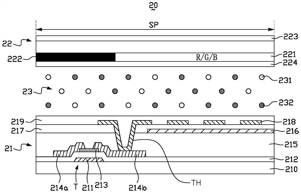
[0032] Please refer to Figure 2 to Figure 5 The first embodiment of the present invention provides a display panel 20 including a first substrate 21 , a second substrate 22 opposite to the first substrate 21 , and a liquid crystal layer 23 between the first substrate 21 and the second substrate 22 .

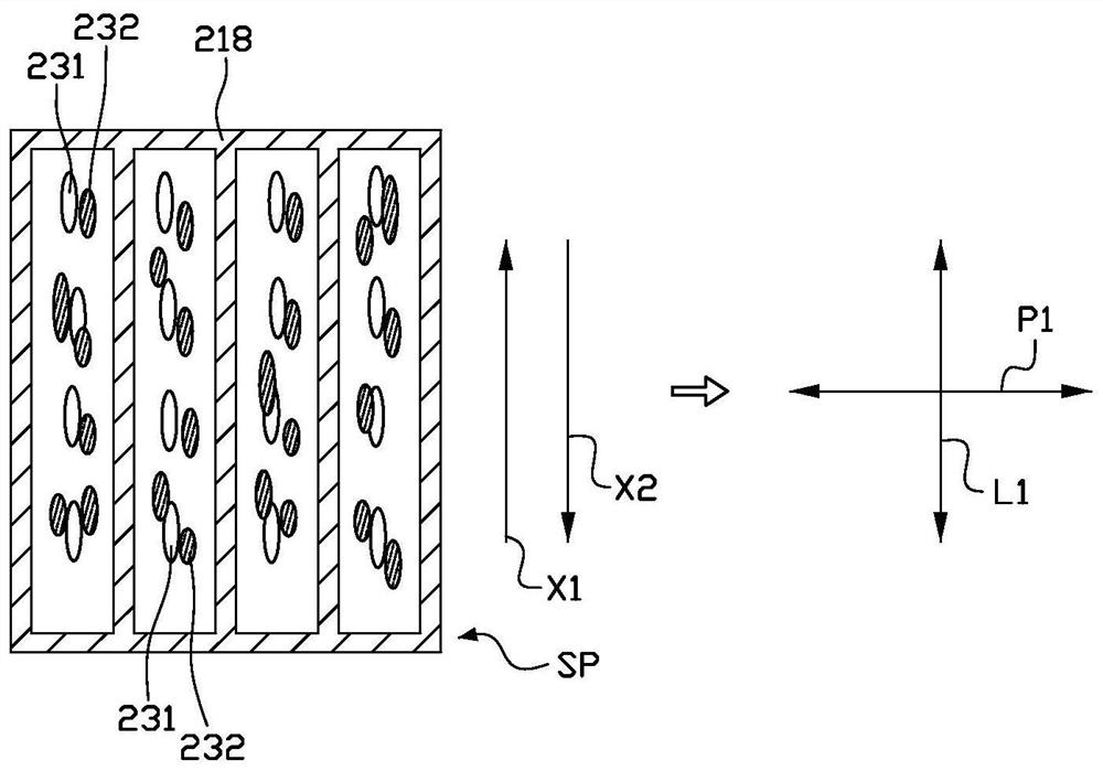
[0033] The first substrate 21 may be a thin film transistor array substrate, and the first substrate 21 is provided with a plurality of scanning lines (not shown), a plurality of data lines (not shown), a plurality of a thin film transistor T, a common electrode 216 and a plurality of pixel electrodes 218. The plurality of scanning lines and the plurality of data lines are insulated and intersect to define and form a plurality of pixel regions SP ( Figure 2 to Figure 5 One of the pixel regions SP is shown in . Each pixel region SP is provided with a thin film transistor T and a pixel electrode 218 , and the pixel electrode 218 is connected to the corresponding scan line and d...

no. 2 example

[0055] Please refer to Figure 6 to Figure 9 The second embodiment of the present invention provides a display panel 20 including a first substrate 21 , a second substrate 22 opposite to the first substrate 21 , and a liquid crystal layer 23 between the first substrate 21 and the second substrate 22 . The first substrate 21 may be a thin film transistor array substrate, and the second substrate 22 may be a color filter substrate.

[0056] The main difference between this embodiment and the above-mentioned first embodiment is that the pixel electrode 218 and the common electrode 216 are respectively located on different substrates, wherein the pixel electrode 218 is formed on the first substrate 21 and the common electrode 216 is formed on the second substrate 22 . For other structures of this embodiment, reference may be made to the foregoing first embodiment, and details are not repeated here.

[0057] Such as Figure 6 and Figure 7 As shown, when no voltage is applied be...


PUM

PropertyMeasurementUnit
lengthaaaaaaaaaa

Abstract

A display panel (20) and a display device. A display panel (20), comprising a first substrate (21), a second substrate (22), and a liquid crystal layer (23) located between the first substrate (21) and the second substrate (22), the first substrate (21) A plurality of pixel regions (SP) are formed on the liquid crystal layer (23), the liquid crystal layer (23) contains liquid crystal molecules (231), the first alignment layer (219) is arranged on the first substrate (21) close to the liquid crystal layer (23), and the second substrate ( 22) is provided with a second alignment layer (224) close to the liquid crystal layer (23), and a polarizer (223) is provided on the outside of the second substrate (22). The polarizer (223) has a light transmission axis (P1), and the first The first alignment direction (X1) of the alignment layer (219) and the second alignment direction (X2) of the second alignment layer (224) are antiparallel, and both are in the direction of the light transmission axis (P1) of the polarizer (223) Vertically, the liquid crystal layer (23) is doped with quantum rods (232), and in each pixel region (SP), quantum rods (232) with different sizes are mixed with liquid crystal molecules (231), and the liquid crystal molecules ( 231) are arranged along the first alignment direction (X1) and the second alignment direction (X2), the alignment direction of the quantum rods (232) is consistent with the liquid crystal molecules (231), and the quantum rods (232) can convert the incident non-polarized light Converts to linearly polarized light in the same direction as its long axis.

Description

technical field [0001] The present invention relates to the field of display technology, in particular to a display panel and a display device with the display panel. Background technique [0002] Liquid crystal display (LCD) has the advantages of good image quality, small size, light weight, low driving voltage, low power consumption, no radiation and relatively low manufacturing cost, and occupies a dominant position in the field of flat panel display. [0003] Such as figure 1 as shown, figure 1 is a schematic cross-sectional view of a typical existing liquid crystal display device, and the liquid crystal display device includes a display panel 40 and a backlight unit 50 . The display panel 40 includes an array substrate 41, a color filter substrate 42, and a liquid crystal layer 43 sandwiched between the array substrate 41 and the color filter substrate 42, and an upper polarizer 44 is arranged above the color filter substrate 42. , a lower polarizer 45 is provided be...

Claims


Application Information

Patent Timeline
Patent Type & Authority Patents(China)
IPC IPC(8): G02F1/1337G02F1/1333G02F1/1343
CPCG02F1/1337G02F1/1333G02F1/134309G02F1/133773
Inventor 柯中乔段周雄刘味李红侠荣誉东陶圆龙
Owner KUSN INFOVISION OPTOELECTRONICS
Why Eureka
Try Eureka