Patterned color conversion film and display device using same
A display device and conversion film technology, which is applied in lighting devices, optics, light sources, etc., can solve problems such as uneven viewing angles, achieve high light extraction rate, improve backlight utilization rate, and high backlight utilization rate.
- Summary
- Abstract
- Description
- Claims
- Application Information
AI Technical Summary
Problems solved by technology
Method used
Image
Examples
Embodiment 1
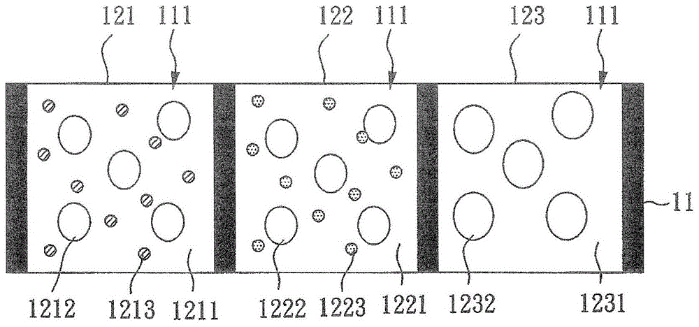
[0057] Such as figure 1 As shown, this embodiment provides a patterned color conversion film applied to blue light as a backlight (or light source), including: a separator 11 with a plurality of openings 111; and red pixel units 121, green pixel units 122 and the transparent pixel unit 123 are respectively disposed in the opening 111 . Wherein, the red pixel unit 121 and the green pixel unit 122 respectively include: substrates 1211, 1221, scattering particles 1212, 1222 dispersed in the substrates 1211, 1221, and quantum dots 1213, 1223 dispersed in the substrates 1211, 1221, and transparent The pixel unit 123 includes: a matrix 1231 and scattering particles 1232 dispersed in the matrix 1231 .
[0058] In the patterned color conversion film of this embodiment, the material of the matrix 1211 , 1221 , 1231 can be a material known in the art, and is preferably a material with a refractive index of 1.4˜1.7. Specific examples of usable materials for the matrix such as silicone ...
Embodiment 2
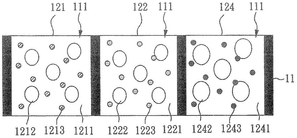
[0070] Such as image 3As shown, this embodiment provides a patterned color conversion film applied to ultraviolet light as a backlight source (or light source), including: a separator 11 with a plurality of openings 111; and red pixel units 121, green pixel units The unit 122 and the blue pixel unit 124 are respectively disposed in the opening 111 . Wherein, the red pixel unit 121, the green pixel unit 122 and the blue pixel unit 124 respectively include: substrates 1211, 1221, 1241, scattering particles 1212, 1222, 1242 dispersed in the substrates 1211, 1221, 1241, and dispersed in the substrate 1211 , 1221, 1241 quantum dots 1213, 1223, 1243 in .
[0071] In simpler terms, also compare figure 1 and image 3 The difference between this embodiment and the first embodiment is that the transparent pixel unit 123 of the first embodiment is replaced by the blue pixel unit 124 .
[0072] In this embodiment, the material and refractive index of the substrates 1211 , 1221 , 1241...
Embodiment 3
[0076] This embodiment provides a liquid crystal display device using the patterned color conversion film provided in Embodiment 1.
[0077] Such as Figure 4 As shown, the liquid crystal display device of this embodiment includes: a light emitting source 41 ; and a patterned color conversion film 1 disposed on a light emitting surface of the light emitting source 41 . In addition to the above elements, the liquid crystal display device of this embodiment also includes: a first polarizer 42 arranged on the light source 41; a first substrate 43 arranged on the first polarizer 42, and on the first substrate 43 A first electrode 431 and a first alignment layer 432 are arranged in sequence; a second substrate 45 is provided with a second electrode 451 and a second alignment layer 452 in sequence on one side, and the first alignment layer 432 and the first alignment layer Two alignment layers 452 are disposed opposite to each other; a liquid crystal layer 44 is disposed between th...
PUM
| Property | Measurement | Unit |
|---|---|---|
| particle diameter | aaaaa | aaaaa |
| particle diameter | aaaaa | aaaaa |
| thickness | aaaaa | aaaaa |
Abstract
Description
Claims
Application Information


