Pixel structure, manufacturing method and display panel

a manufacturing method and display panel technology, applied in the field of display technology, can solve the problems of shortening the lift increasing the power consumption of the display panel, and becoming an urgent problem, so as to reduce the power consumption of the display device, increase the light extraction rate of the light emitting device, and prolong the life

Inactive Publication Date: 2018-07-12
TCL CHINA STAR OPTOELECTRONICS TECH CO LTD
View PDF5 Cites 6 Cited by
  • Summary
  • Abstract
  • Description
  • Claims
  • Application Information

AI Technical Summary

Benefits of technology

[0020]The beneficial effect of the present invention is: comparing to the conventional art, in the pixel structure of the present invention, through irradiating the liquid prepolymers such that the liquid prepolymers spontaneously form the concave-convex structure film layer. Then, manufacturing the protection layer and the pixel electrode layer having a same concave-convex structure as the concave-convex structure film layer in order to form a pixel structure in order to increase a light extraction rate of the light emitting device, decrease the power consumption of the display device and extend the life.

Problems solved by technology

However, because of the optical loss inside the structure of the device, only 20% of the emitted light of the device is used so as to greatly increase the power consumption of the display panel, and shorten the lift of the display device.
The above situations have become an urgent problem required to be solved by the industry.

Method used


Image

  • Pixel structure, manufacturing method and display panel
  • Pixel structure, manufacturing method and display panel
  • Pixel structure, manufacturing method and display panel

Examples


Embodiment Construction

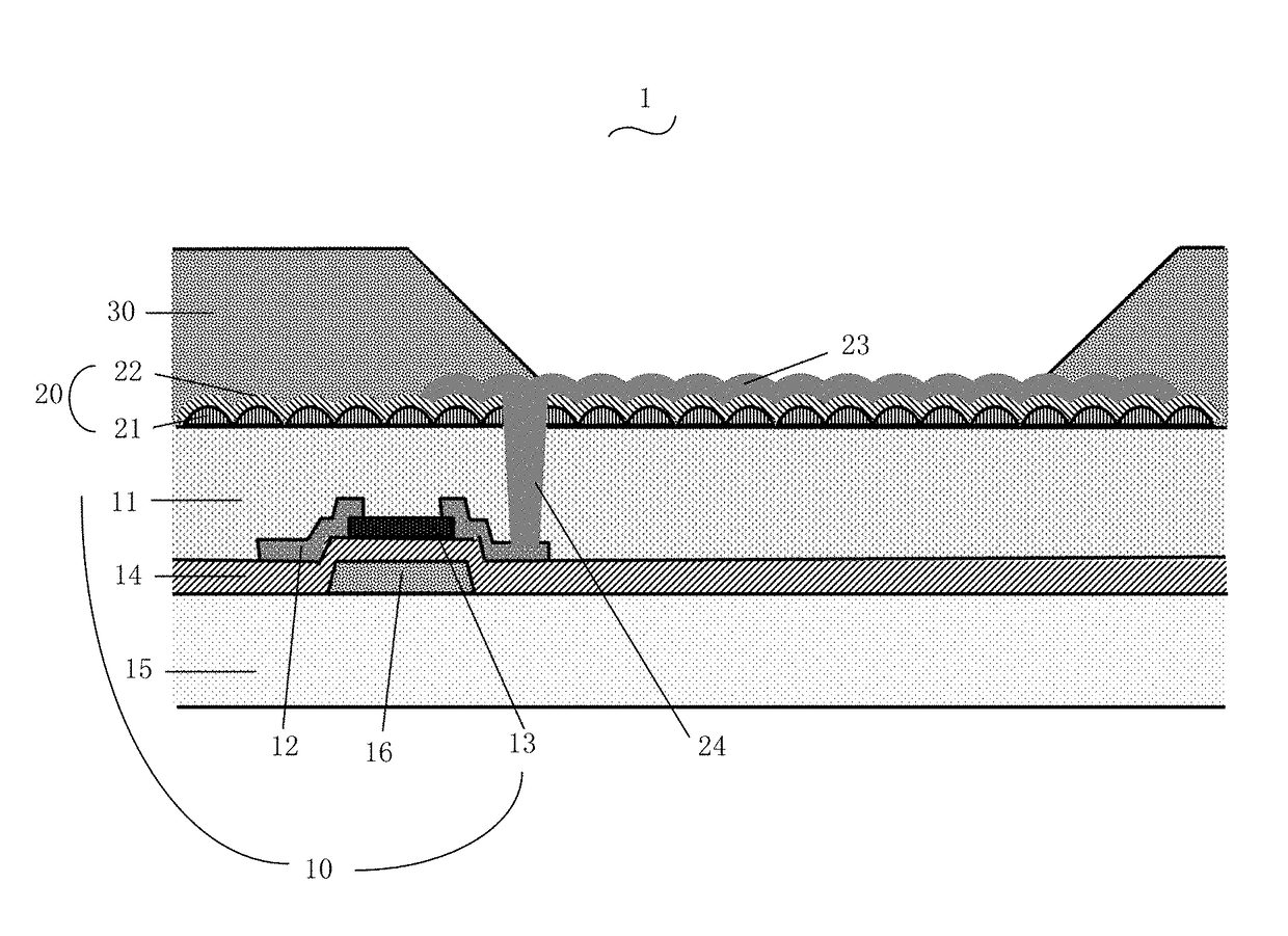
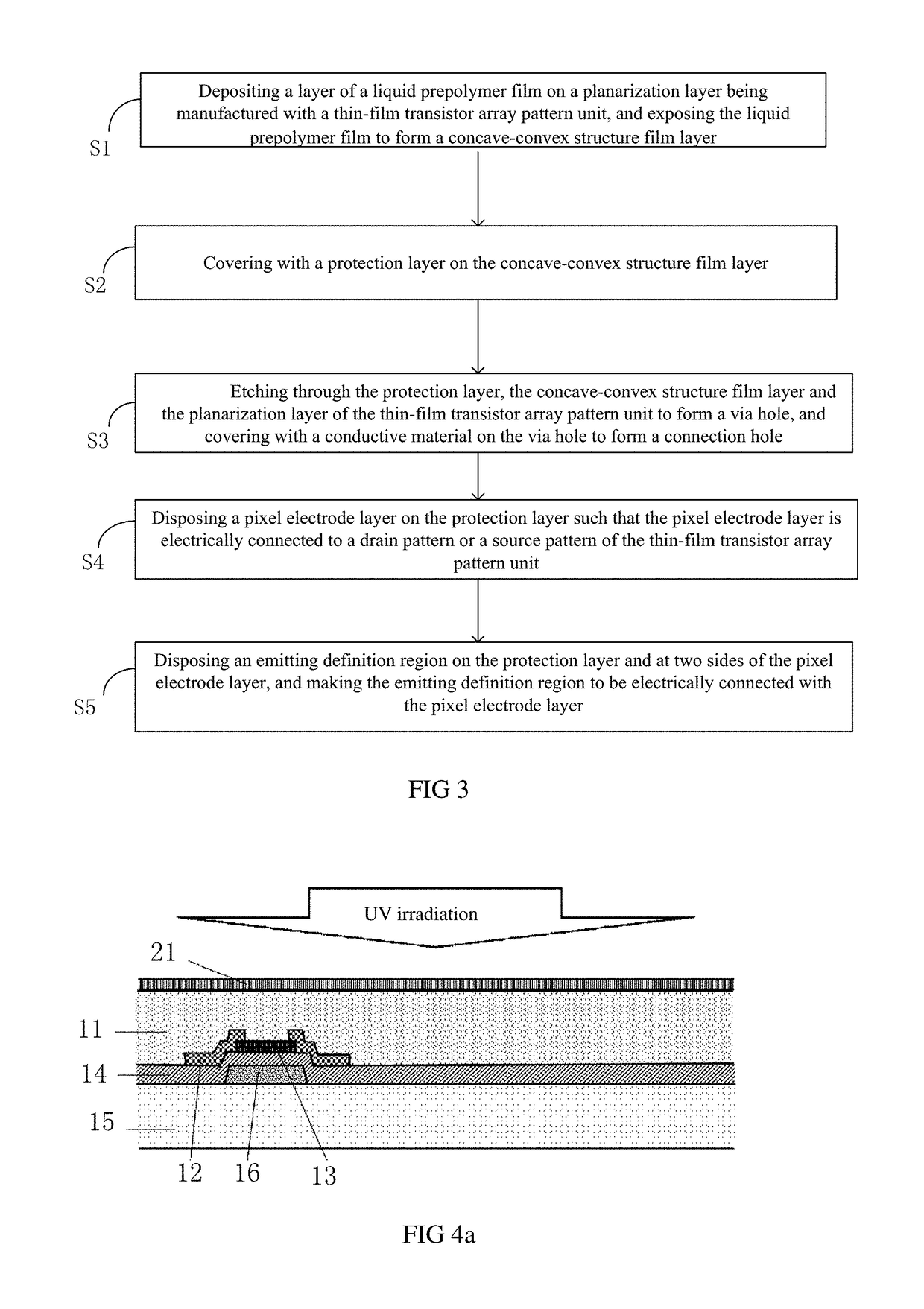
[0026]With reference to FIG. 1, and FIG. 1 is a schematic diagram of a pixel structure of the present invention. As shown in FIG. 1, the pixel structure 1 includes a thin-film transistor array pattern unit 10 and a pixel pattern unit 20 which are stacked. The pixel pattern unit 20 includes a concave-convex structure film layer 21 disposed on the thin-film transistor array pattern unit 10, a protection layer 22 covered on the concave-convex structure film layer 21, a pixel electrode layer 23 located on the protection layer 22, and electrically connected to the thin-film transistor array pattern unit 10 and an emitting definition region 30.

[0027]Wherein, the thin-film transistor array pattern unit 10 includes a planarization layer 11 for supporting the concave-convex structure film layer 21, a source pattern and a drain pattern 12 disposed on the planarization layer 11 and are separated, an active layer 13 electrically connected between the source pattern and the drain pattern 12, a g...


PUM


Abstract

A pixel structure, a manufacturing method and a display panel are provided. The pixel structure comprises a thin-film transistor array pattern unit and a pixel pattern unit which are disposed stacked; the pixel pattern unit includes a concave-convex structure film layer disposed on the thin-film transistor array pattern unit, a protection layer covered on the concave-convex structure film layer, a pixel electrode layer located on the protection layer, and electrically connected to the thin-film transistor array pattern unit and an emitting definition region so as to increase a light extraction rate of the light emitting device, decrease the power consumption of the display device and extend the life.

Description

BACKGROUND OF THE INVENTION1. Field of the Invention[0001]The present invention relates to a display technology field, and more particularly to a pixel structure, a manufacturing method and a display panel.2. Description of Related Art[0002]Currently, the importance of the display adopted for visible information transmission media is further strengthened. In order to dominate the future market, the display is developed toward a lighter, thinner, lower power, lower cost and better image quality trend. The organic electroluminescent diode (OLED) has advantages of self-luminous, fast response, wide viewing angle, high brightness, light and so on, the potential market prospect is optimistic by the industry. The quantum dot light emitting diode (QLED) has advantages of light color purity, high luminescence quantum efficiency, easy to adjust the light color and so on such that the QLED has become a powerful competitor of the OLED. The above two display technology is two main developing di...

Claims


Application Information

Patent Timeline
Patent Type & Authority Applications(United States)
IPC IPC(8): H01L27/12H01L29/786H01L29/423H01L23/522H01L21/311
CPCH01L27/1248H01L29/78618H01L29/42384H01L23/5226H01L27/1262H01L21/31111H01L27/156H01L33/06H01L27/3246H01L27/3258H01L27/3248H01L51/502H01L2227/323H01L27/3262H01L27/1218H10K59/121H01L25/0753H10K59/123H10K59/124H10K59/122H10K50/858H10K59/879H10K50/115H10K59/1201H10K59/1213
Inventor SHI, WEN
Owner TCL CHINA STAR OPTOELECTRONICS TECH CO LTD
Why Eureka
Try Eureka