Sapphire-substrate single-electrode LED chip structure and preparation method thereof

A sapphire substrate and LED chip technology, which is applied in circuits, electrical components, semiconductor devices, etc., can solve the problems of restricting the light extraction rate of small-sized chips, achieve the effect of reducing the proportion of electrode area and improving the light extraction rate

Inactive Publication Date: 2016-02-24
JIANGSU XINGUANGLIAN SEMICON
View PDF4 Cites 7 Cited by
  • Summary
  • Abstract
  • Description
  • Claims
  • Application Information

AI Technical Summary

Problems solved by technology

[0002] With the improvement of epitaxy and chip technology, the performance of LED devices is gradually improved, and the size of the device is gradually reduced. The positive and negative electrodes of the chip cannot be separated due to the precision and process limit requirements of the wire bonding process. The limit is reduced, the smaller the device size, the larger the area ratio of electrodes, which seriously restricts the light extraction rate of small-sized chips

Method used


Image

  • Sapphire-substrate single-electrode LED chip structure and preparation method thereof
  • Sapphire-substrate single-electrode LED chip structure and preparation method thereof
  • Sapphire-substrate single-electrode LED chip structure and preparation method thereof

Examples


Embodiment 1

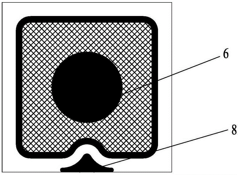
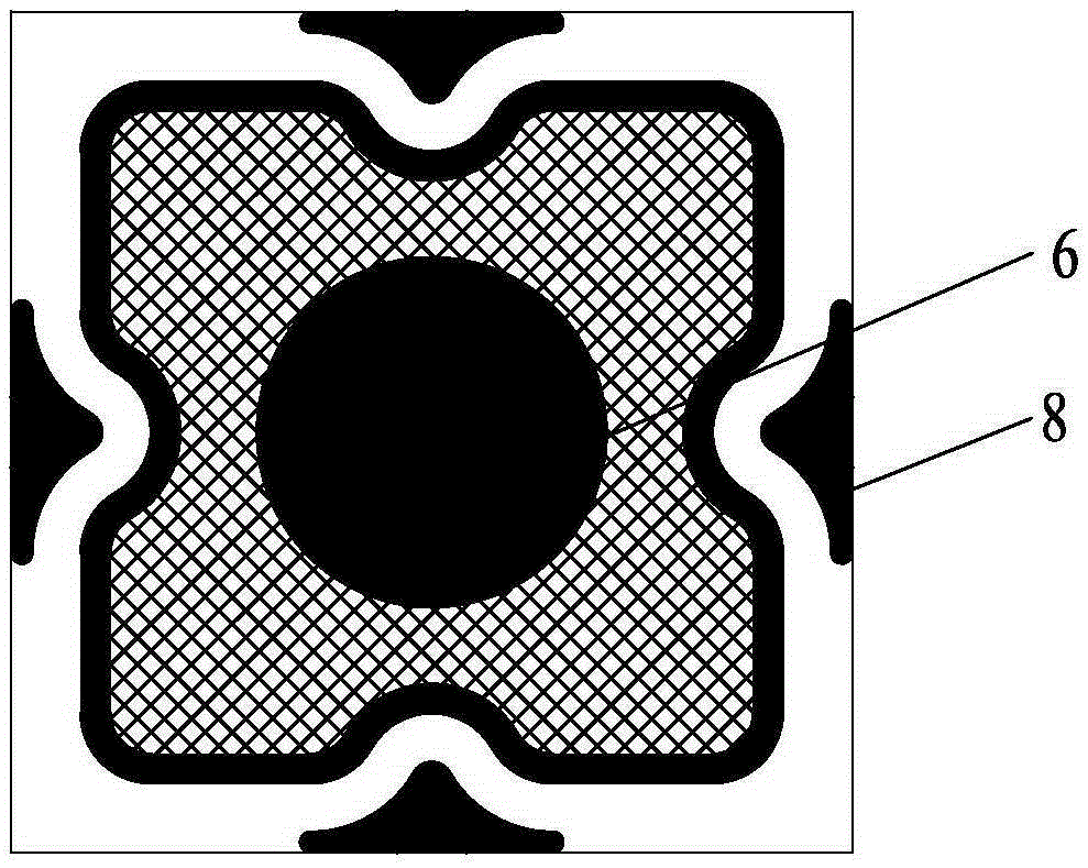
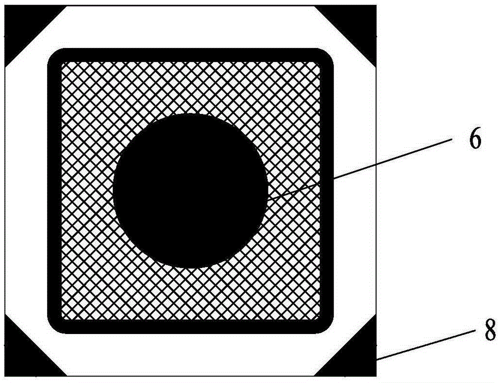
[0039] Such as Figure 1 ~ Figure 3 , Figure 7 As shown, the sapphire substrate single-electrode LED chip structure of the present invention includes a sapphire substrate 1, and an epitaxial structure layer is grown on the sapphire substrate 1, and the epitaxial structure layer includes a U-GaN layer 2, an N-GaN layer 3, an MQW layer 4 and the P-GaN layer 5, the MQW layer 4 and the P-GaN layer 5 are partially etched to expose the N-GaN layer 3, an ITO layer 9 is provided on the P-GaN layer 5, and a positive electrode 6 is provided on the ITO layer 9; One side of the sapphire substrate 1 (such as figure 1 shown), multiple sides (such as figure 2 shown) or multiple sides (such as image 3 As shown), the inclined grooves 7 are arranged respectively, the inclined grooves 7 extend from the upper surface of the N-GaN layer 3 to the lower surface of the sapphire substrate 1, and the inclined grooves 7 are half or 1 / 4 of a conical hole; The sidewall of the chute 7 is covered wit...

Embodiment 2

[0048] Such as Figure 4 ~ Figure 6 , Figure 10 As shown, the sapphire substrate single-electrode LED chip structure of the present invention includes a sapphire substrate 1, and an epitaxial structure layer is grown on the sapphire substrate 1, and the epitaxial structure layer includes a U-GaN layer 2, an N-GaN layer 3, an MQW layer 4 and the P-GaN layer 5, the MQW layer 4 and the P-GaN layer 5 are partially etched to expose the N-GaN layer 3, an ITO layer 9 is provided on the P-GaN layer 5, and a positive electrode 6 is provided on the ITO layer 9; One side of the sapphire substrate 1 (such as Figure 4 shown) or multiple sides (such as Figure 5 As shown), a slanted groove 7 is provided, and the slanted groove 7 extends from the upper surface of the N-GaN layer 3 into the sapphire substrate 1 , and the side wall of the slanted groove 7 is covered with a metal layer with a thickness of 1-5 μm to form a negative electrode 8 .

[0049]The preparation method of the sapphir...


PUM


Abstract

The invention relates to a sapphire-substrate single-electrode LED chip structure and a preparation method thereof. The sapphire-substrate single-electrode LED chip structure comprises a sapphire substrate. Epitaxial structural layers are grown on the sapphire substrate. The epitaxial structural layers include a U-GaN layer, an N-GaN layer, an MQW layer and a P-GaN layer. The MQW layer and a P-GaN layer are partially etched, and the N-GaN layer is exposed. An ITO layer is arranged on the P-GaN layer. A positive electrode is arranged on the ITO layer. The sapphire-substrate single-electrode LED chip structure is characterized in that negative electrodes are arranged on the side surfaces of the sapphire substrate, the negative electrodes are arranged in a skewed slot of one side surface or skewed slots of a plurality of side surfaces or side edges, and metal 1-5 [mu]m in thickness covers side walls of the skewed slots to form the negative electrodes. According to the invention, the area ratio of the electrodes is greatly lowered, and the light extraction rate of the chip is effectively improved.

Description

technical field [0001] The invention relates to a sapphire substrate single-electrode LED chip structure and a preparation method thereof, belonging to the technical field of semiconductors. Background technique [0002] With the improvement of epitaxy and chip technology, the performance of LED devices is gradually improved, and the size of the device is gradually reduced. The positive and negative electrodes of the chip cannot be separated due to the precision and process limit requirements of the wire bonding process. The smaller the limit, the smaller the device size, the larger the area ratio of the electrodes, which seriously restricts the light extraction rate of small-sized chips. Contents of the invention [0003] The purpose of the present invention is to overcome the deficiencies in the prior art, provide a sapphire substrate single-electrode LED chip structure and its preparation method, greatly reduce the electrode area ratio, and effectively improve the light...

Claims


Application Information

Patent Timeline
Patent Type & Authority Applications(China)
IPC IPC(8): H01L33/38H01L33/00
CPCH01L33/385H01L33/007
Inventor 黄慧诗张秀敏郑宝玉
Owner JIANGSU XINGUANGLIAN SEMICON
Why Eureka
Try Eureka