Wafer processing method

Active Publication Date: 2005-03-17
DISCO CORP
View PDF11 Cites 6 Cited by
  • Summary
  • Abstract
  • Description
  • Claims
  • Application Information

AI Technical Summary

Benefits of technology

[0008] It is an object of the present invention to provide a wafer processing method having high productivity and capable of dividing a wafer without reducing the brightness of an optical device.
[0019] In the present invention, as the grooves formed along the dividing lines in the back surface of the wafer by the laser beam application step are removed by carrying out the grinding step after the wafer has been divided, the brightness of the optical devices is not reduced. In the present invention, since the wafer is cut along the grooves formed along the dividing lines, there is no cutting margin unlike cutting with a cutting blade. Therefore, the area ratio of the dividing lines to the optical device can be reduced and productivity can be thereby improved.

Problems solved by technology

Since a sapphire substrate, silicon carbide substrate, or the like has a high Mohs hardness, cutting with the above cutting blade is not always easy.
Therefore, in the case of an optical device measuring, for example, about 300 μm×300 μm, there is a problem that the area ratio of the dividing lines to the optical device is large, thereby reducing productivity.
When a laser beam is applied to the front surface of a wafer to process it, however, heat energy is concentrated on the exposed area to produce debris that stick fast to the front surface of the wafer, thereby greatly reducing the quality of optical devices.
When the deteriorated layer is formed by applying a laser beam with its focusing point on the center portion of the inside of the area to be divided of the wafer, there is a problem that it remains around the optical device, and light emitted from the optical device is absorbed by the deteriorated portion to reduce the brightness of the optical device.

Method used


Image

  • Wafer processing method
  • Wafer processing method
  • Wafer processing method

Examples


first embodiment

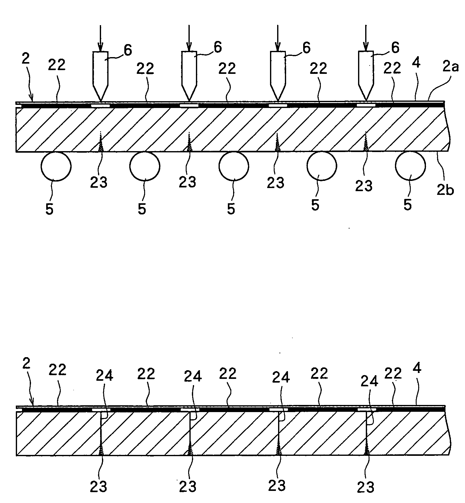
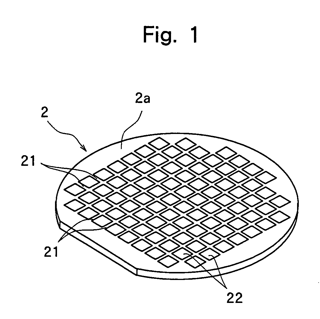
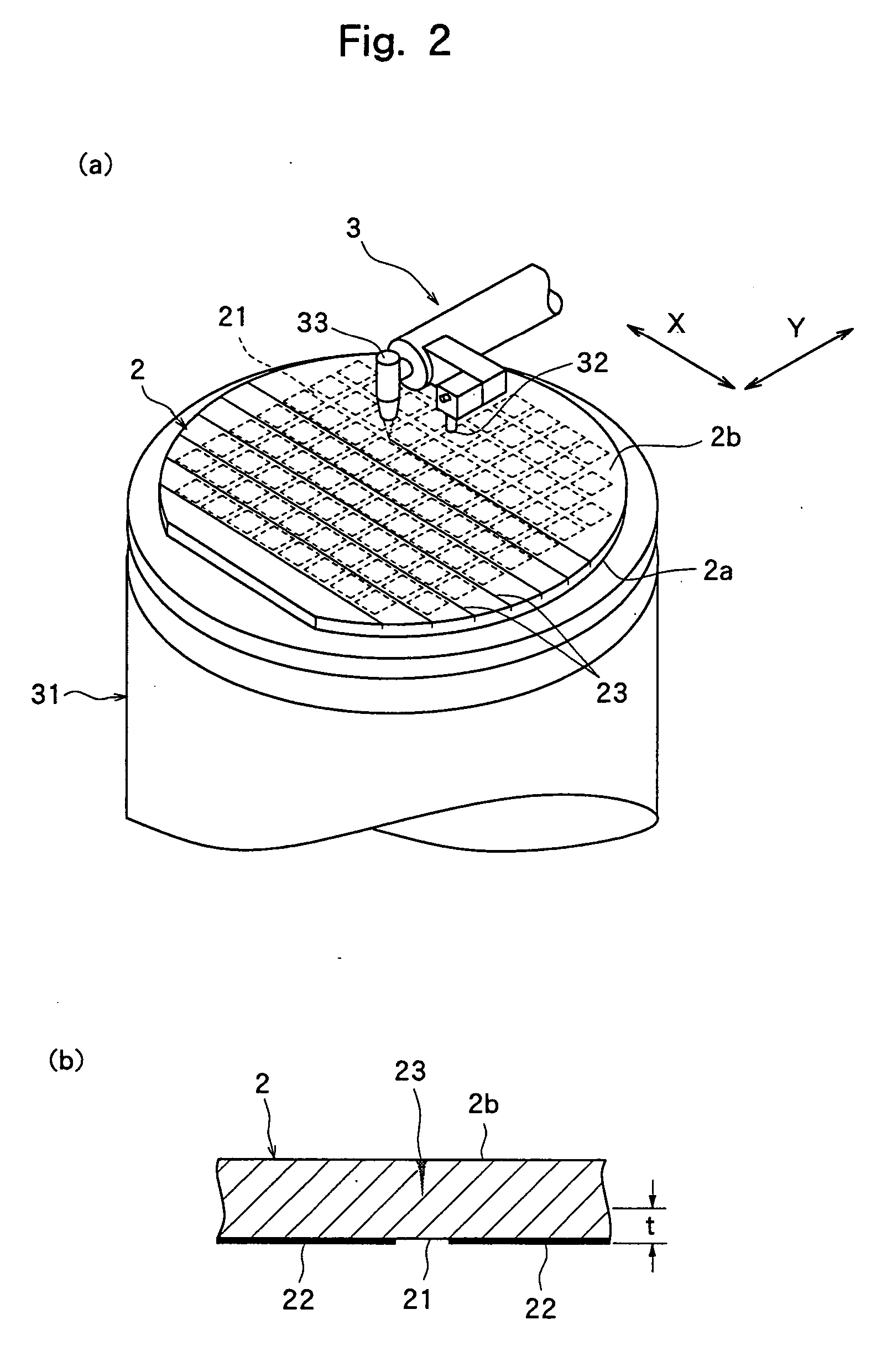
[0026]FIG. 1 is a perspective view of an optical device wafer 2 to be divided according to the present invention. In the optical device wafer 2 shown in FIG. 1, a plurality of dividing lines 21 are formed in a lattice pattern on the front surface 2a thereof, and optical devices 22 in which a gallium nitride-based compound semiconductor and the like is laminated are formed in a plurality of areas sectioned by the dividing lines 21. This optical device wafer 2 has the optical devices 22 measuring 0.3 mm×0.3 mm formed on the surface of a sapphire substrate having a diameter of 2 inches and a thickness of 430 μm in the illustrated embodiment. The processing method for dividing this optical device wafer 2 into individual optical devices 22 will be described with reference to FIGS. 2 to 5.

[0027] In the first embodiment, the step of applying a laser beam to the above optical device wafer 2 along the dividing lines 21 from the side of the back surface 2b thereof to form grooves having a pr...

second embodiment

[0040] The processing method for dividing the optical device wafer 2 into individual optical devices 22 will be described hereinbelow.

[0041] In the second embodiment, the order of the above laser beam application step and the protective sheet affixing step in the first embodiment is reversed. That is, in the second embodiment, the step of affixing the protective sheet 4 to the front surface 2a of the optical device wafer 2 is first carried out. Then, the optical device wafer 2 having the protective sheet 4 affixed to the front surface 2a is held on the chuck table 31 of the laser beam processing machine 3 in such a manner that the back surface 2b faces up as shown in FIG. 2(a) to carry out the above laser beam application step. After the protective sheet affixing step and the laser beam application step are carried out, the dividing step and the grinding step in the first embodiment are carried out likewise in the second embodiment.


PUM


Abstract

A wafer processing method for dividing a wafer having optical devices that are formed in a plurality of areas sectioned by dividing lines formed in a lattice pattern on the front surface, along the dividing lines, which comprises a laser beam application step of applying a laser beam to the wafer along the dividing lines from the side of back surface thereof to form grooves having a predetermined depth in the back surface; a protective sheet affixing step of affixing a protective sheet to the front surface of the wafer having the grooves in the back surface; a dividing step of dividing the wafer having the protective sheet affixed to the front surface along the grooves; and a grinding step of grinding the back surface of the wafer divided along the grooves in a state of the protective sheet being affixed to the wafer, to remove the grooves.

Description

FIELD OF THE INVENTION [0001] The present invention relates to a wafer processing method for dividing a wafer having optical devices that are formed in a plurality of areas sectioned by dividing lines (streets) formed in a lattice pattern on the front surface, along the dividing lines. DESCRIPTION OF THE PRIOR ART [0002] A wafer having optical devices comprising a gallium nitride-based compound semiconductor which are formed in a plurality of areas sectioned by dividing lines (streets) formed in a lattice pattern on the front surface of a sapphire substrate and the like is divided along the dividing lines into individual optical devices such as light emitting diodes or laser diodes which are widely used in electric equipment. This wafer is generally divided by a cutting machine called “dicer”. The cutting machine comprises a chuck table for holding a workpiece such as a semiconductor wafer or optical device wafer, a cutting means for cutting the workpiece held on the chuck table, an...

Claims


Application Information

Patent Timeline
IPC IPC(8): B23K26/364B23K26/40B23K101/40H01L21/301H01L21/304H01L21/78
CPCB23K26/367B23K26/4075H01L21/78B24B37/042B23K2201/40B23K26/40B23K26/364B23K2101/40B23K2103/50
Inventor NAGAI, YUSUKEAOKI, MASASHIHOSHINO, HITOSHI
Owner DISCO CORP
Why Eureka
Try Eureka