Thin film transistor substrate for flat panel display

a thin film transistor and substrate technology, applied in the direction of basic electric elements, electrical equipment, semiconductor devices, etc., can solve the problems of difficult to ensure the stability of the thin film transistor, the oxide semiconductor layer may be easily affected by the light intruding from the outside, and the deformation of the oxide semiconductor layer, etc., to achieve superior video quality, reduce the load of the data line, and increase the density. the effect of ultra high density

Active Publication Date: 2018-03-01
LG DISPLAY CO LTD
View PDF2 Cites 6 Cited by
  • Summary
  • Abstract
  • Description
  • Claims
  • Application Information

AI Technical Summary

Benefits of technology

[0021]In order to overcome the above mentioned drawbacks, a purpose of the present disclosure is to provide a thin film transistor substrate for a large and / or ultra high density flat panel display. Another purpose of the present disclosure is to provide a thin film transistor substrate for a flat panel display having superior video quality in which the load of the data line is reduced by removing or minimizing the parasitic capacitance formed at the crossing point between the scan line and the data line. Still another purpose of the present disclosure is to provide a thin film transistor substrate for a flat panel display in which the aperture ratio is maximized by minimizing the size of the thin film transistor. Yet another purpose of the present disclosure is to provide a thin film transistor substrate for a flat panel display in which the characteristics of the thin film transistor is not degraded or changed even though any manufacturing tolerance is occurred during the manufacturing process.
[0029]The thin film transistor substrate for flat panel display according to the present disclosure has the structure in which a buffer layer and / or a gate insulating layer are further added to the intermediated insulating layer between the scan line and the data line. Therefore, the parasitic capacitance between the scan line and the data line would be minimized of eliminated. As a result, the load to the data line is reduced and the resistance of the data line is lowered. It can get the superior effect for the high speed driving of the organic light emitting diodes. Further, as the thin film transistor is disposed as overlapping with the scan line, the size of the thin film transistor is minimized. It can get the merits for increasing the aperture ratio by reducing the area ratio of the thin film transistor in the pixel area. In addition, the sizes of the parasitic capacitances of the thin film transistors are similar each other, even though there are manufacturing errors are occurred during the manufacturing process. Therefore, the characteristics of the thin film transistors may be evenly controlled over the large area as to keep the originally designed purpose. The large area and ultra high density flat panel display according to the present disclosure provides a superior video property.

Problems solved by technology

When the lights radiated from the organic light emitting layer are intruded into the oxide semiconductor layer of the thin film transistor, it is hard to ensure the stability of the thin film transistor.
However, when the top gate structure is applied to the bottom emission type organic light emitting diode display, the channel layer is disposed under the gate electrode so that the oxide semiconductor layer may be easily affected and degraded by the lights intruded from the outside.

Method used


Image

  • Thin film transistor substrate for flat panel display
  • Thin film transistor substrate for flat panel display
  • Thin film transistor substrate for flat panel display

Examples


first embodiment

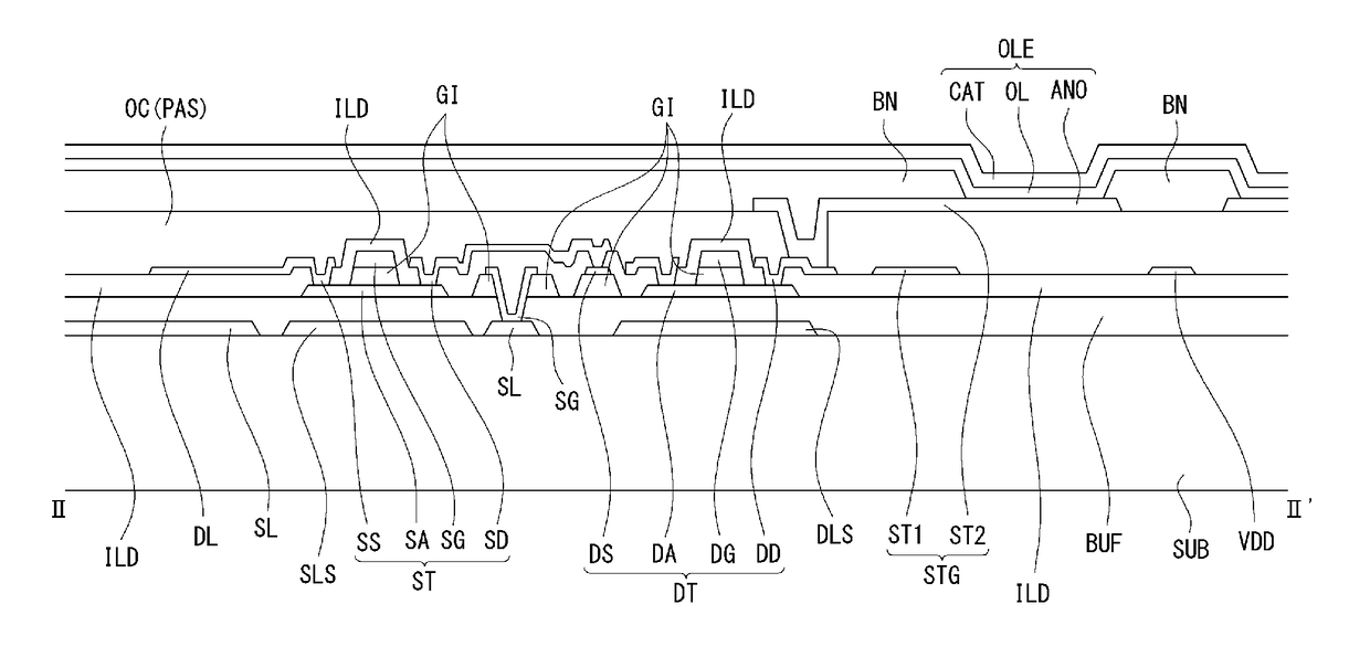
[0048]Referring to FIGS. 5 and 6, a first embodiment of the present disclosure will be described. FIG. 5 is a plane view illustrating the structure of one pixel in the organic light emitting diode display according to the first embodiment of the present disclosure. FIG. 6 is a cross sectional view, along the cutting line II-IP in FIG. 5, illustrating the structure of the organic light emitting diode display according to the first embodiment.

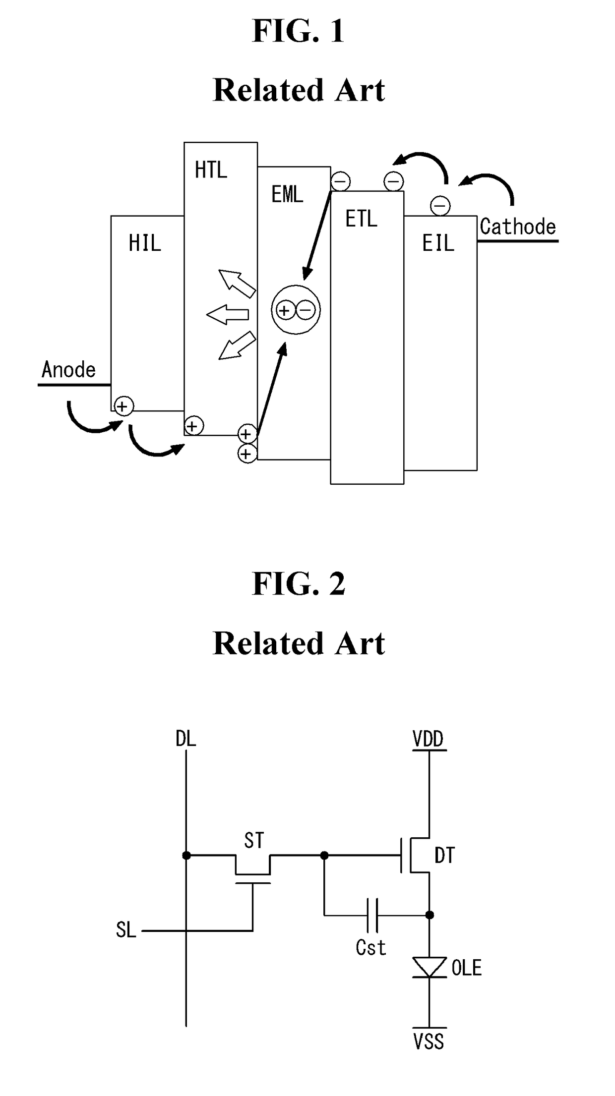
[0049]The organic light emitting diode display according to the first embodiment of the present disclosure comprises a switching thin film transistor ST, a driving thin film transistor DT connected to the switching thin film transistor ST, and an organic light emitting diode OLE connected to the driving thin film transistor DT. The switching thin film transistor ST is disposed at the portion where a scan line SL and a data line DL are crossing. The switching thin film transistor ST acts for selecting the pixel which is connected to the switching ...

second embodiment

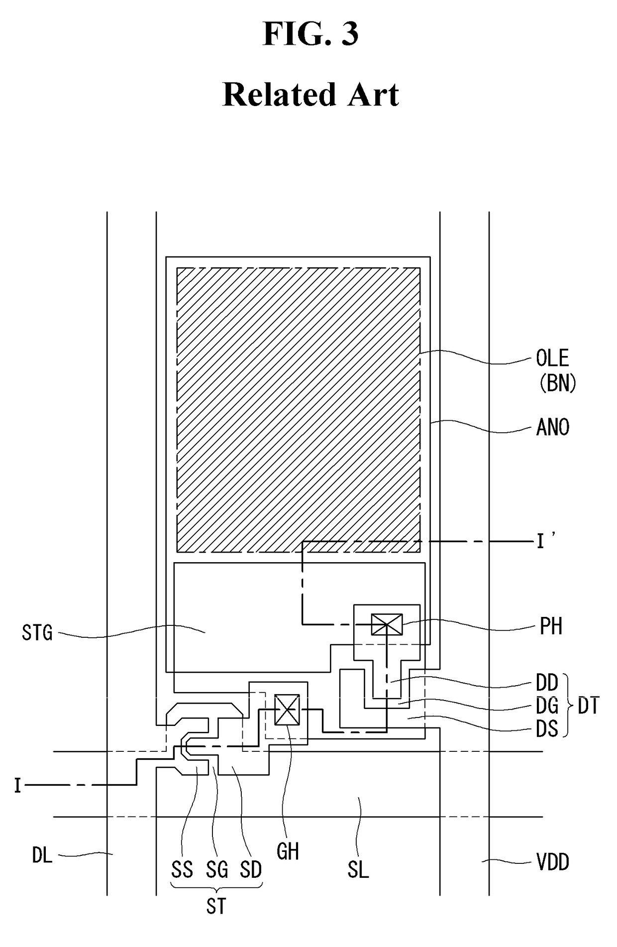
[0067]In the first embodiment, the switching thin film transistor has the structure in which the gate electrode is extruded from the scan line SL. Therefore, as the pixel size is getting smaller (i.e., as the higher resolution), the area ratio of the switching thin film transistor in the pixel area is getting larger.

[0068]In the second embodiment, in order to minimize the area for the switching thin film transistor, a structure is provided in which the gate electrode is defined in some portions of the scan line itself. The organic light emitting diode display according to the second embodiment has the structure in which the non emission area ratio in one pixel area is minimized with an ultra high density resolution (UHD rate or more).

[0069]Hereinafter, the structure of the switching thin film transistor in the organic light emitting diode display will be explained. Further, in the cross sectional view, only the switching thin film transistor is illustrated. However, the thin film tr...

third embodiment

[0078]In the second embodiment, the structure is provided in which the scan line SL and the gate electrode SG are overlapped with respect to each other to form the double gate structure. The scan line SL has much wider width than the gate electrode SG. This is for ensuring that the line resistance of the scan line SL is not increased. However, due to the gate-source parasitic capacitance Cgs formed where the source area of the semiconductor layer SA and the scan line SL are overlapped, and the gate-drain parasitic capacitance Cgd formed where the drain area and the scan line SL, it may be hard to maintain the exact characteristics of the thin film transistor.

[0079]In FIG. 7, the channel area is the area where the semiconductor layer SA and the gate electrode SG are overlapped, illustrated as having the 45° hatch pattern. At the upper area and the lower area of the channel area, there are the areas where the semiconductor layer SA and the scan line SL are overlapped, illustrated as h...


PUM


Abstract

The present disclosure relates to a thin film transistor substrate for flat panel display including an organic light emitting diode display. The present disclosure provides a device comprising: a substrate; a scan line extending in a first direction on the substrate; a buffer layer on the scan line; a semiconductor layer extending in a second direction and crossing the scan line on the buffer layer; a gate insulating layer on the semiconductor layer; a gate electrode connected to the scan line, and extending in the first direction and crossing the semiconductor layer on the gate insulating layer; an intermediate insulating layer on the gate electrode; a data line crossing the scan line on the intermediate insulating layer; a source electrode branching from the data line and contacting a first side of the semiconductor layer; and a drain electrode facing the source electrode and contacting a second side of the semiconductor layer.

Description

[0001]This application claims the benefit of Korea Patent Application No. 10-2016-0111613 filed on Aug. 31, 2016, which is incorporated herein by reference for all purposes as if fully set forth herein.BACKGROUNDTechnical Field[0002]The present disclosure relates to a thin film transistor substrate for flat panel display including an organic light emitting diode display. Especially, the present disclosure relates to a thin film transistor substrate for a large and / or ultra high density flat panel display in which the parasitic capacitance is reduced and it is driven in high speed by increasing the insulating property between the scan line and the data line.Description of the Related Art[0003]Nowadays, various flat panel displays (or ‘FPD’) are developed for overcoming many drawbacks of the cathode ray tube (or ‘CRT’) which is heavy and bulky. The flat panel display devices include the liquid crystal display device (or ‘LCD’), the field emission display (FED), the plasma display pane...

Claims


Application Information

Patent Timeline
Patent Type & Authority Applications(United States)
IPC IPC(8): H01L27/32
CPCH01L27/3279H01L27/3262H01L27/3272H01L29/78633H01L27/124H01L29/7869H01L27/1225H10K59/1315H10K59/1213H10K59/131H01L29/78648H10K59/126H01L27/1274H01L29/78606H01L29/78618
Inventor JEONG, ILGICHO, KYUNGHYUNLEE, SUWOONGHONG, SUNGJIN
Owner LG DISPLAY CO LTD
Why Eureka
Try Eureka