Light emitting diode array and manufacturing method thereof

一种发光二极管、制造方法的技术,应用在电气元件、电固体器件、电路等方向,能够解决制作流程复杂、很难蚀刻均匀性、蚀刻速率不稳定等问题,达到提高光萃取率的效果

Inactive Publication Date: 2012-11-21
ZHANJING TECH SHENZHEN +1
View PDF7 Cites 7 Cited by
  • Summary
  • Abstract
  • Description
  • Claims
  • Application Information

AI Technical Summary

Problems solved by technology

However, the light generated by the light emitting diode can only be emitted to the outside world when the angle is less than the critical angle. Otherwise, due to internal total reflection, a large amount of light will be lost inside the light emitting diode and cannot be emitted to the outside world, resulting in the loss of the entire light emitting diode array. Low light output rate, low brightness
At present, the technology of using etching to roughen the surface of LEDs to increase the brightness of LEDs is well known to the public. The existing technologies are roughly divided into two types: 1. Using high-temperature acidic liquids (such as sulfuric acid, phosphoric acid, etc.) to treat LEDs The disadvantage of etching is that the etching rate is unstable due to uneven temperature in the liquid, and the tank body needs to be well designed so that the liquid operating at high temperature is not dangerous, so the production cost of the tank body will also be relatively high. High; 2. Use ultraviolet light to irradiate and apply voltage to make semiconductor components react with potassium hydroxide easily, and then achieve the purpose of etching. However, insulators need to be made for protection in operation, electrode lines are laid on the chip, and then energized and illuminated Etching, due to the problem of electrode conductivity, it can only be produced on a small chip, and the production of the entire wafer is limited by the distribution of power, so it is difficult to have good etching uniformity, and the production process is more complicated

Method used


Image

  • Light emitting diode array and manufacturing method thereof
  • Light emitting diode array and manufacturing method thereof
  • Light emitting diode array and manufacturing method thereof

Examples


Embodiment Construction

[0030] The present invention will be further described in detail below in conjunction with the accompanying drawings.

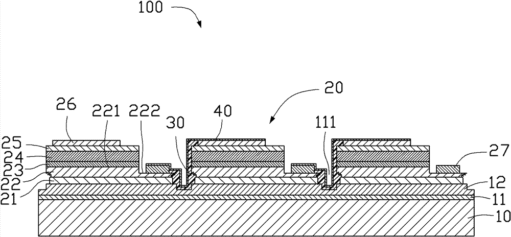
[0031] see figure 1 A light emitting diode array 100 provided in an embodiment of the present invention includes a substrate 10, a plurality of light emitting diodes 20 formed on one side of the substrate 10, an electrical insulating layer 30 between the plurality of light emitting diodes 20, and a The electrical connection wire 40 electrically connected between the plurality of light emitting diodes 20.

[0032] In this embodiment, the light emitting diode array 100 includes three light emitting diodes 20, it can be understood that the number of light emitting diodes 20 in the light emitting diode array 100 is not limited to three, and the specific number can be determined according to the actual required brightness. . Each LED 20 includes a connection layer 21 , an n-type GaN layer 22 , a light emitting layer 23 , a p-type GaN layer 24 , a transparent con...


PUM


Abstract

The invention relates to a light emitting diode array which comprises a substrate and a plurality of light emitting diodes formed at one side of the substrate, wherein the plurality of light emitting diodes are electrically connected; each light emitting diode comprises a connection layer, an n-type gallium nitride layer, a light emitting layer and a p-type gallium nitride layer, which are orderly formed on the substrate; the connection layer can be etched by alkaline solution; the bottom surface of the n-type gallium nitride layer facing to the connection layer is oppositely polarized gallium nitride, and a bared roughened surface is arranged on the bottom surface. The invention also relates to a manufacturing method of the light emitting diode array.

Description

technical field [0001] The invention relates to a semiconductor element, in particular to a light emitting diode array and a manufacturing method thereof. Background technique [0002] Now, light emitting diodes (Light Emitting Diodes, LEDs) have been widely used in lighting and other fields. In order to improve lighting brightness, people often use light emitting diode arrays composed of multiple light emitting diodes in lamps and the like. However, the light generated by the light emitting diode can only be emitted to the outside world when the angle is less than the critical angle. Otherwise, due to internal total reflection, a large amount of light will be lost inside the light emitting diode and cannot be emitted to the outside world, resulting in the loss of the entire light emitting diode array. The light output rate is low and the brightness is not high. At present, the technology of using etching to roughen the surface of LEDs to increase the brightness of LEDs is ...

Claims


Application Information

Patent Timeline
Patent Type & Authority Applications(China)
IPC IPC(8): H01L25/075H01L33/42H01L33/00
CPCH01L27/153H01L33/22H01L33/62H01L2924/0002H01L2924/00
Inventor 洪梓健沈佳辉
Owner ZHANJING TECH SHENZHEN
Why Eureka
Try Eureka