LED and its making method

A technology of light-emitting diodes and manufacturing methods, which is applied to electrical components, circuits, semiconductor devices, etc., and can solve problems such as high process difficulty and low yield rate

Active Publication Date: 2008-07-02
EPISTAR CORP
View PDF1 Cites 7 Cited by
  • Summary
  • Abstract
  • Description
  • Claims
  • Application Information

AI Technical Summary

Problems solved by technology

However, the disadvantage of this U.S. Patent No. 5,376,580 is that the semiconductor is used as the bonding medium, so the alignment of...

Method used


Image

  • LED and its making method
  • LED and its making method
  • LED and its making method

Examples


Embodiment Construction

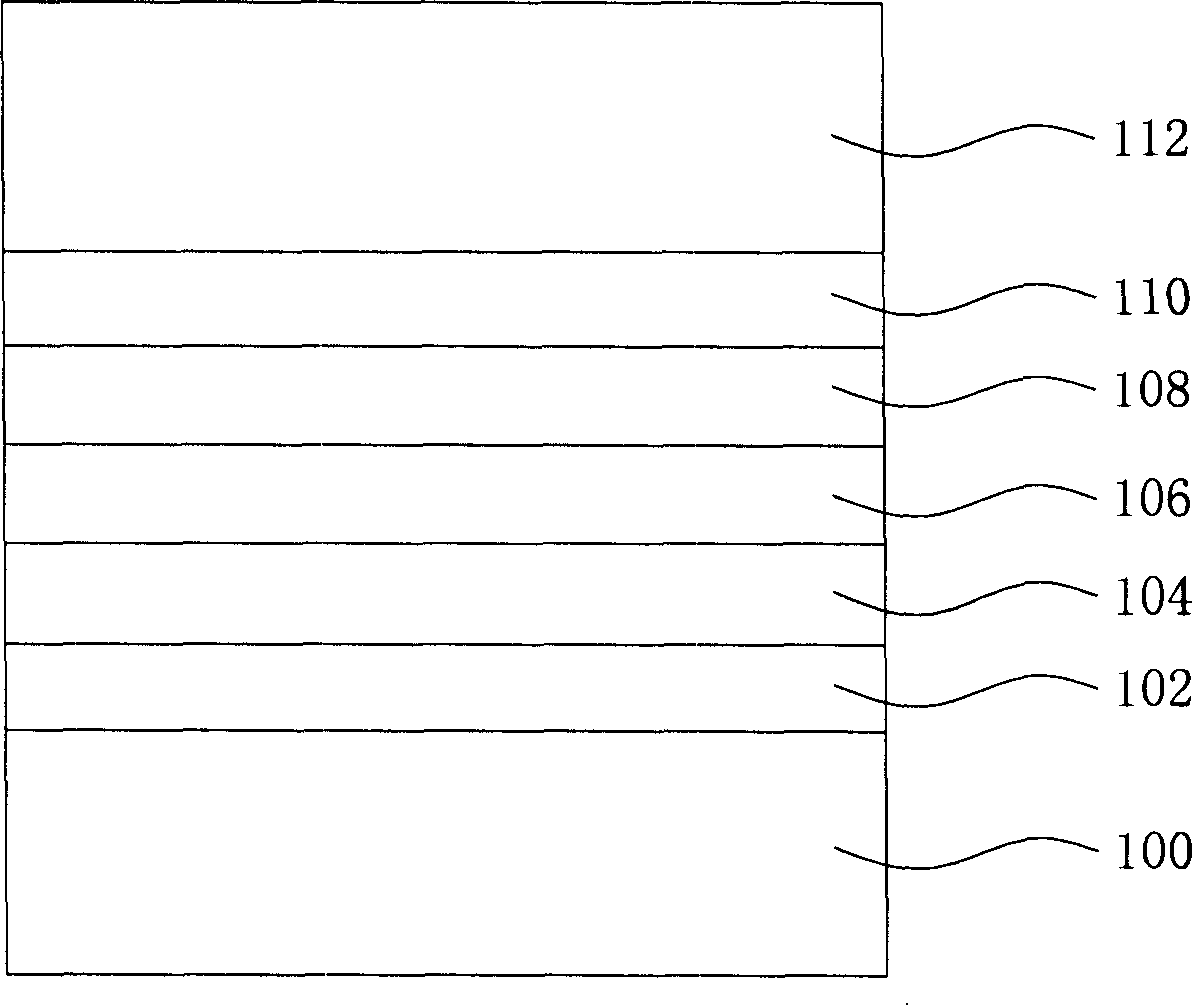
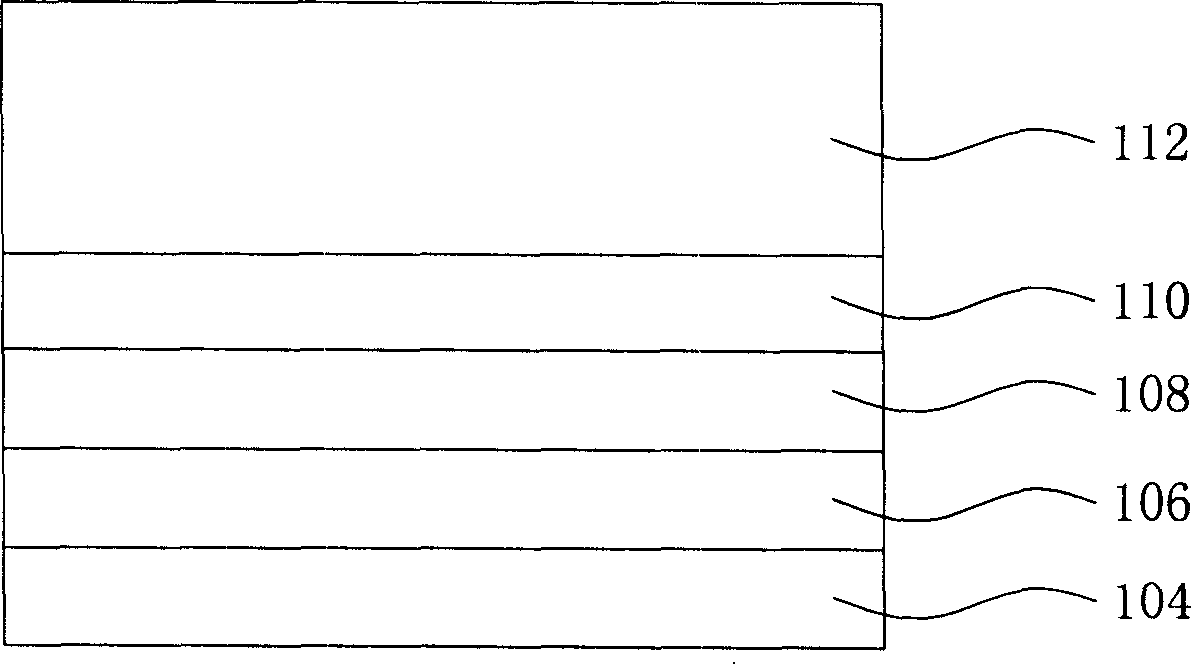
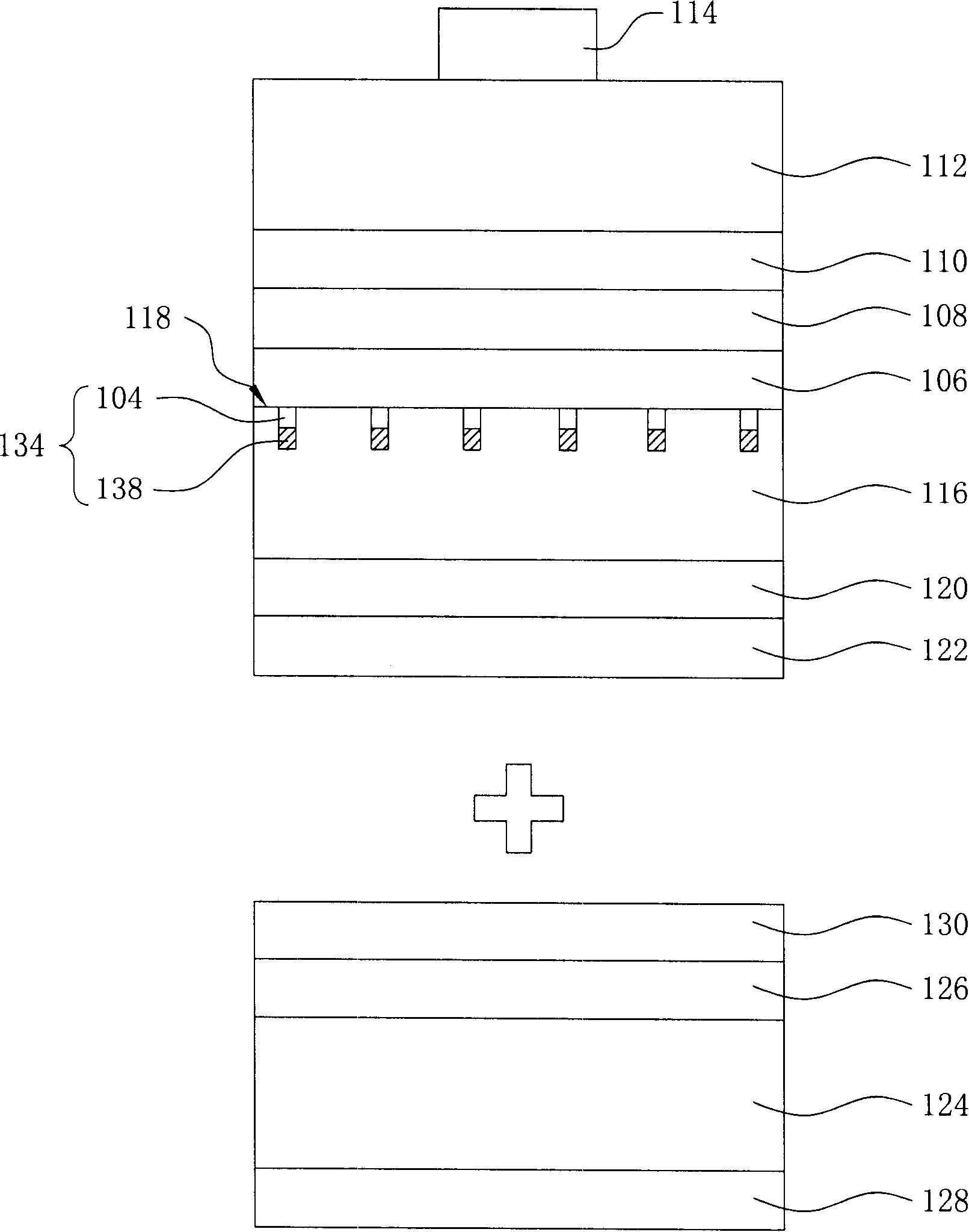
[0014] The invention discloses a light-emitting diode and its manufacturing method, which has a thicker window layer, so that the current diffusion can be enhanced, and the light extraction efficiency can be improved, which is more conducive to the roughening treatment of the surface of the element, and further improves the light extraction rate to achieve an improvement. Efficacy of the luminance of light-emitting diode components. In addition, all necessary processes can be completed before wafer bonding, so the bonding temperature is more flexible, and a wider process window can be obtained. Furthermore, an alloy with a lower melting point can be used as the die bonding medium, thereby improving the reliability of the die bonding process. In order to make the narration of the present invention more detailed and complete, you can refer to the following combination Figure 1 to Figure 4 description of.

[0015] Please refer to Figure 1 to Figure 4 , which is a sectional vie...


PUM

PropertyMeasurementUnit
Thicknessaaaaaaaaaa
Thicknessaaaaaaaaaa

Abstract

The invention relates to a luminescent diode (LED) and a manufacturing method thereof. The LED at least comprises the following processes: a conductive base plate is provided with a first surface relative with a second surface; a metal joint layer is arranged on the first surface of the conductive base plate; a metal reflecting layer is jointed with the metal joint layer; an N type semiconductor layer is arranged on the metal reflecting layer; an active layer is arranged on the N type semiconductor layer; a P type semiconductor layer is arranged on the active layer; a window layer is arranged on the P type semiconductor layer, wherein the thickness of the window layer is above 50Mum and the window layer is composed of transparent conductive material; a P type electrode is arranged on the window layer.

Description

technical field [0001] The present invention relates to a light-emitting diode (LED) and its manufacturing method, and in particular to a high-efficiency light-emitting diode and its manufacturing method. Background technique [0002] In the production of light-emitting diodes, III-V semiconductor compounds, such as gallium nitride (GaN), aluminum gallium nitride (AlGaN), indium gallium nitride (InGaN), and aluminum indium gallium nitride (AlInGaN) and other materials, is a fairly common material. Such light-emitting epitaxial structures composed of III-V semiconductor compounds are mostly grown on non-conductive sapphire substrates, which are different from conductive substrates used in other light-emitting devices. Since the sapphire substrate is an insulator, electrodes cannot be directly fabricated on the sapphire substrate. Therefore, when making the electrodes of the light-emitting diodes composed of III-V semiconductor compounds, the electrodes must be directly in c...

Claims


Application Information

Patent Timeline
IPC IPC(8): H01L33/00
Inventor 许世昌洪详竣魏世祯苏住裕
Owner EPISTAR CORP
Why Eureka
Try Eureka