Manufacturing method of micro LED display panel and display panel
A display panel and manufacturing method technology, applied in the direction of electrical components, electrical solid devices, circuits, etc., can solve the problems of reduced work efficiency, decreased work efficiency, increased time, etc., and achieve the effect of reducing installation accuracy requirements and improving installation efficiency
- Summary
- Abstract
- Description
- Claims
- Application Information
AI Technical Summary
Problems solved by technology
Method used
Image

Examples
Embodiment 1
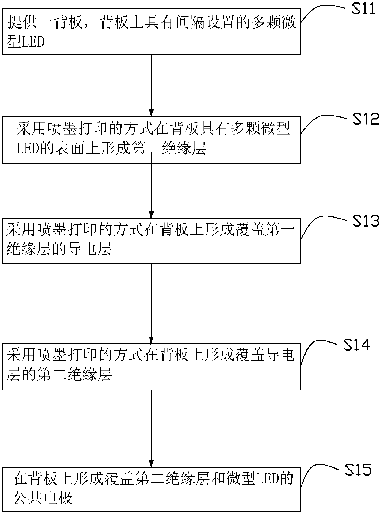
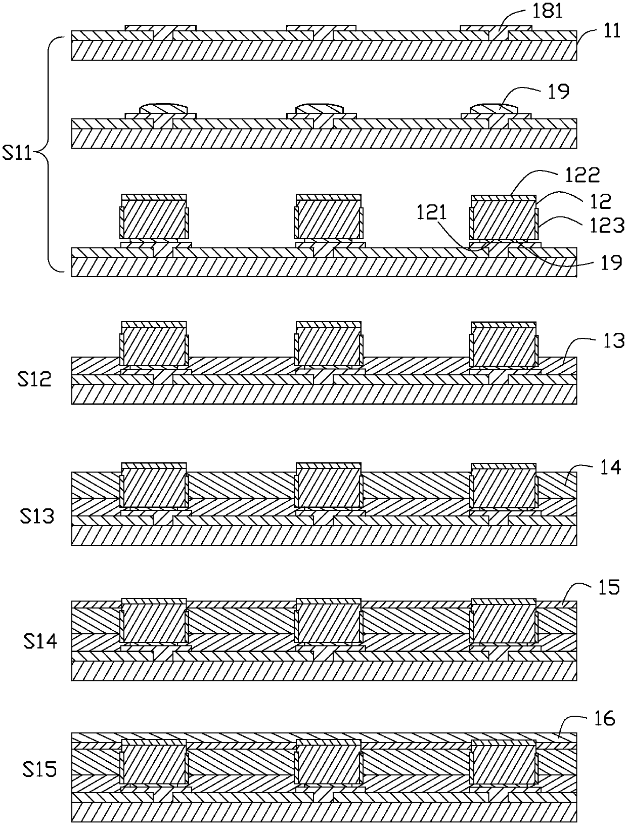
[0060] The manufacturing method of the micro-LED display panel provided in this embodiment, such as figure 1 shown, including:
[0061] Step S11 , providing a backboard with a plurality of micro LEDs arranged at intervals.
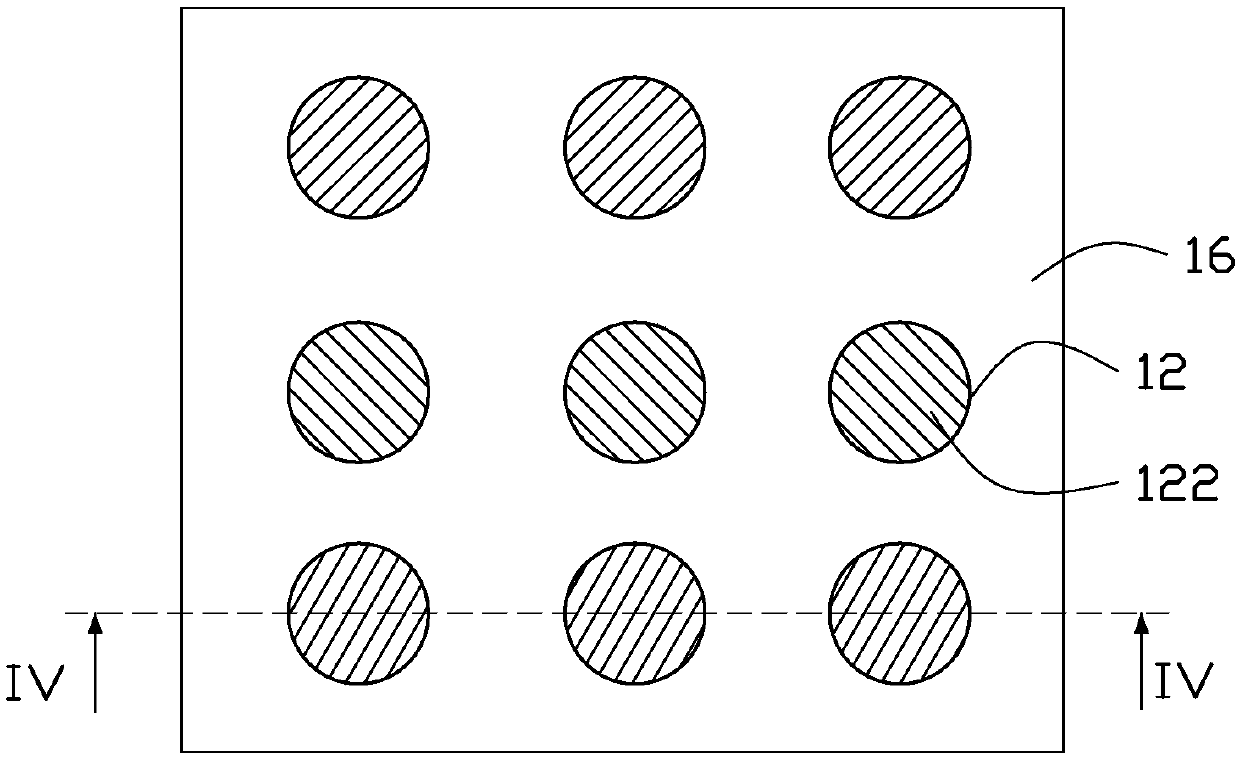
[0062] Specifically, such as figure 2As shown, the backplane 11 includes a plurality of first driving elements 181 arranged at intervals. Step S11 specifically includes: depositing solder 19 on the backplane 11, each solder 19 is correspondingly arranged on one first driving element 181, and a plurality of The micro-LEDs 12 are transferred to the solder 19 on the backplane 11 . Each micro-LED 12 includes a lower electrode 121 and an upper electrode 122, and each micro-LED 12 corresponds to a solder 19. The above-mentioned solder 19 can make the first driving element 181 below it electrically connected to the lower electrode 121 of the micro-LED 12 above it. connected, the corresponding micro LED 12 can be driven to emit light through the first driving ...
Embodiment 2
[0077] The manufacturing method of the micro-LED display panel provided in this embodiment, its process is as follows Figure 5 with Image 6 shown. Figure 5 The illustrated method includes the following steps.
[0078] Step S21, such as Image 6 As shown, a backboard 11 is provided, the backboard has a plurality of micro-LEDs 12 arranged at intervals, and a plurality of first driving elements 181 corresponding to the micro-LEDs 12 are arranged on the backboard 11. Specifically, step S21 and implementation Step S11 in Example 1 is the same, and reference may be made to the above description.
[0079] Further, such as Image 6 , in step S22, a first partition wall 171 is formed on the backplane 11; the first partition wall 171 divides the micro-LED display panel into a plurality of mutually independent light-emitting regions, and each of the light-emitting regions A miniature LED 12 is arranged inside.
[0080] Further, after forming the first partition wall 171, a plura...
Embodiment 3
[0103] The manufacturing method of the micro-LED display panel provided by the second embodiment of the present invention, such as Figure 10 shown.
[0104] Wherein, steps S31 and S32 are as described in the second embodiment, and will not be repeated here.
[0105] Please also refer to Figure 10 with Figure 11 , in step S33, forming a second isolation wall 172 in each of the light emitting regions. Specifically, a second partition wall 172 is arranged in each of the above-mentioned light-emitting regions, and the second partition wall 172 is arranged between the first partition wall 171 and the micro LED 12 in the light-emitting region where it is located, and the second driving element 182 is disposed between the first isolation wall 171 and the second isolation wall 172 in the light emitting region, so that the second driving element 182 can be exposed to contact with the subsequently formed conductive layer 14 . The height of the second partition wall 172 should be ...
PUM
 Abstract
Description
Claims
Application Information
 - R&D
- Intellectual Property
- Life Sciences
- Materials
- Tech Scout
- Unparalleled Data Quality
- Higher Quality Content
- 60% Fewer Hallucinations
Browse by: Latest US Patents, China's latest patents, Technical Efficacy Thesaurus, Application Domain, Technology Topic, Popular Technical Reports.
© 2025 PatSnap. All rights reserved.Legal|Privacy policy|Modern Slavery Act Transparency Statement|Sitemap|About US| Contact US: help@patsnap.com