A butt coupling method for monolithic integrated chips

A single-chip integration and docking coupling technology, applied in the field of docking coupling, can solve the problems of low coupling efficiency affecting the optical power of the device, affecting the transmission characteristics of the device, and poor refractive index, so as to improve the quality of docking coupling, improve growth quality, and reduce loss Effect

Active Publication Date: 2021-02-26
湖北光安伦芯片有限公司
View PDF7 Cites 0 Cited by
  • Summary
  • Abstract
  • Description
  • Claims
  • Application Information

AI Technical Summary

Problems solved by technology

Traditional docking methods, such as the patent US7018861B2, cannot solve two major problems. One is that the thickness of the materials in different functional areas is inconsistent, and the centers of the active areas of the two need to be completely aligned to avoid the mismatch of optical fields in different functional areas, which will cause low coupling efficiency and affect the device. The second is that the connection of different functional materials not only requires a smooth connection interface to reduce loss, but also there is a difference in refractive index at the connection interface that will cause light reflection and affect the transmission characteristics of the device such as chirp

Method used


Image

  • A butt coupling method for monolithic integrated chips
  • A butt coupling method for monolithic integrated chips
  • A butt coupling method for monolithic integrated chips

Examples


Embodiment Construction

[0040] The solutions of the present invention will be further described below in conjunction with the accompanying drawings and embodiments.

[0041] This embodiment discloses a butt coupling method for monolithic integrated chips, including the following steps:

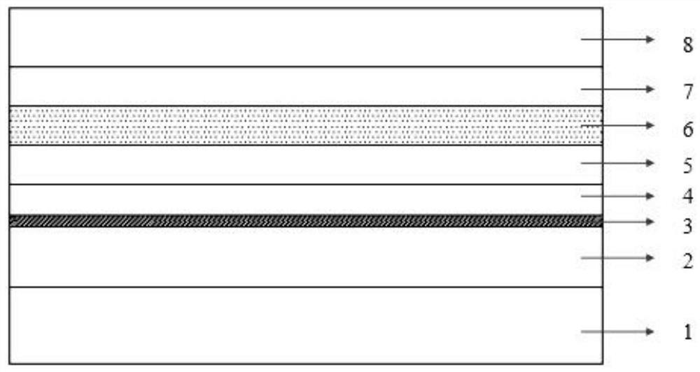
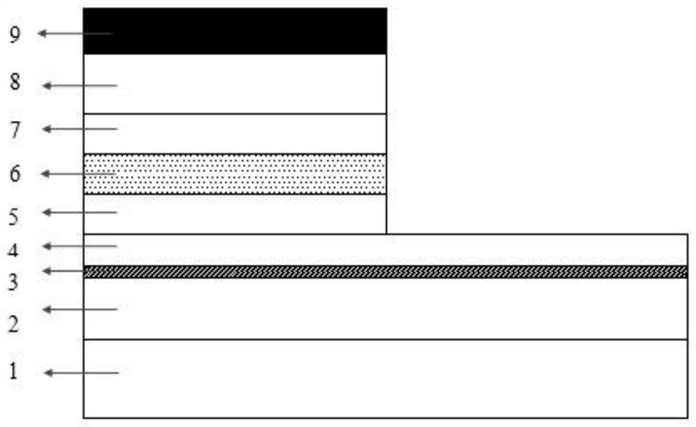
[0042] S1) if figure 1 , growing the first functional device on the substrate 1, including sequentially growing the first InP buffer layer 2, the quaternary optical field control layer 3, the second InP buffer layer 4, the first lower waveguide layer 5, and the first active quantum well Layer 6, first upper waveguide layer 7, first InP cladding layer 8;

[0043] Among them, the material composition of the quaternary optical field control layer 3 is 120-180nm different from the PL of the active MQW, and its function is to control the optical field of the first functional device in the active / passive waveguide of the second functional device to avoid The light leakage of the substrate can be used as an etching stop l...


PUM

PropertyMeasurementUnit
thicknessaaaaaaaaaa
heightaaaaaaaaaa
angleaaaaaaaaaa

Abstract

The invention discloses a butt coupling method for monolithic integrated chips, comprising: S1, producing a first active functional device on a substrate, the device divides an InP buffer layer into two parts through an optical field control layer, and through Control the growth thickness of the second buffer layer to achieve complete alignment between the center of the active area of ​​the first functional device and the center of the active area of ​​the second functional device; S2, deposit a dielectric thin film, and define the second functional device by photolithography. The end of the mask and the direction of the optical waveguide form a certain angle to reduce the reflection at the interface between the first functional device and the second functional device; S3, use etching and selective etching to remove part of the first functional device; S4, heat the first functional device to Heat treatment to form a smooth side wall interface and a certain length of undercut; S5, butt growth of the second functional device. It has high coupling efficiency and good transmission characteristics.

Description

technical field [0001] The invention relates to monolithic integrated chip technology, in particular to a butt coupling method for monolithic integrated chips, which is used in the manufacturing process of monolithic integrated chips. Background technique [0002] The main purpose of monolithic photonic integrated chips is to monolithically integrate at least two functional devices, including integration between active devices, such as semiconductor lasers, semiconductor optical amplifiers, electroabsorber modulators, semiconductor photodetectors, and Integration of active and passive devices, such as optical waveguides, multimode interferometers, mode spot converters, gratings, etc. Compared with discrete devices, monolithic integrated devices can complete more complex functions than discrete devices through the combination of components, which greatly reduces the coupling cost and packaging cost of different devices, and is excellent in optical, electrical performance, sta...

Claims


Application Information

Patent Timeline
Patent Type & Authority Patents(China)
IPC IPC(8): H01S5/026
CPCH01S5/0261H01S2304/04
Inventor 王汉华黄爽许海明刘建军唐琦
Owner 湖北光安伦芯片有限公司
Why Eureka
Try Eureka