Supercharge Your Innovation With Domain-Expert AI Agents!

Electronic device

A technology of electronic devices and circuit boards, which is applied in the direction of instruments, character and pattern recognition, and print image acquisition, can solve the problems of increased assembly tolerance, increased manufacturing cost, and decreased assembly yield and quality, so as to reduce assembly tolerance and reduce The effect of processing

Pending Publication Date: 2020-07-24
EGIS TECH
View PDF0 Cites 0 Cited by
  • Summary
  • Abstract
  • Description
  • Claims
  • Application Information

AI Technical Summary

Problems solved by technology

However, this method will cause the appearance of the steel plate to be processed in accordance with the middle frame structure, which will increase the manufacturing cost
Moreover, due to the large number of processing times, the assembly tolerance is increased, resulting in a decline in assembly yield and quality

Method used


Image

  • Electronic device
  • Electronic device
  • Electronic device

Examples


Embodiment Construction

[0037] Embodiments of the present invention will be described in detail below in conjunction with the accompanying drawings. It is to be understood that the appended drawings are for purposes of description and explanation, not of limitation. Components may not be shown to scale for clarity. In addition, some components and / or component symbols may be omitted in some drawings. In the specification and drawings, the same or similar component symbols are used to designate the same or similar components. When it is described that a component is "disposed on", "connected to" ... another component, without special limitation, the component may be "directly disposed on", "directly connected to" ... another component, and there may also be an intermediary components. It is contemplated that elements and features of one embodiment, where practicable, can be incorporated to advantage in another embodiment without further elaboration.

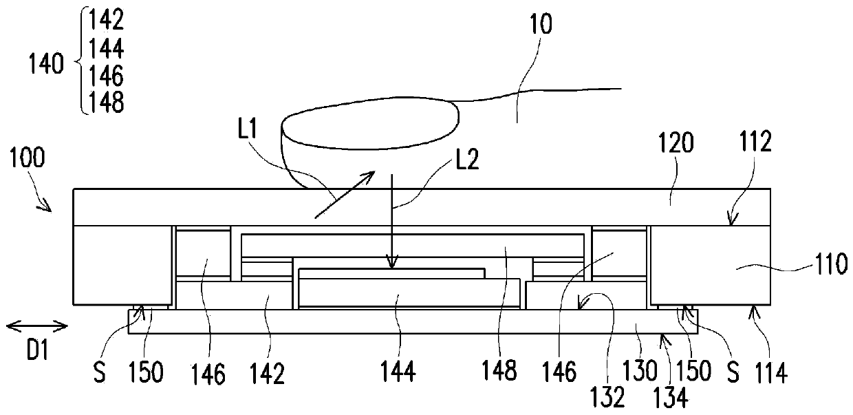
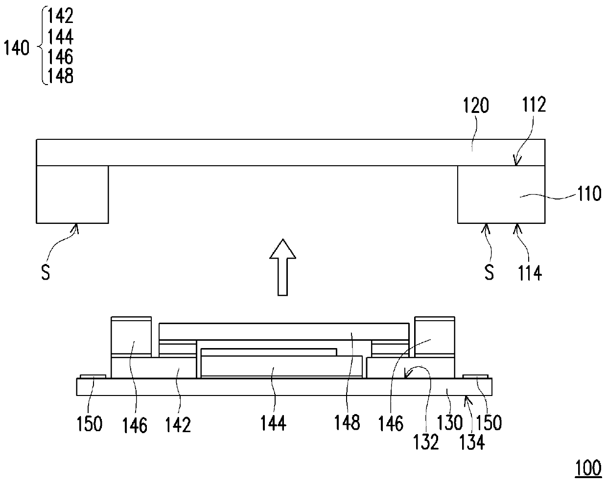
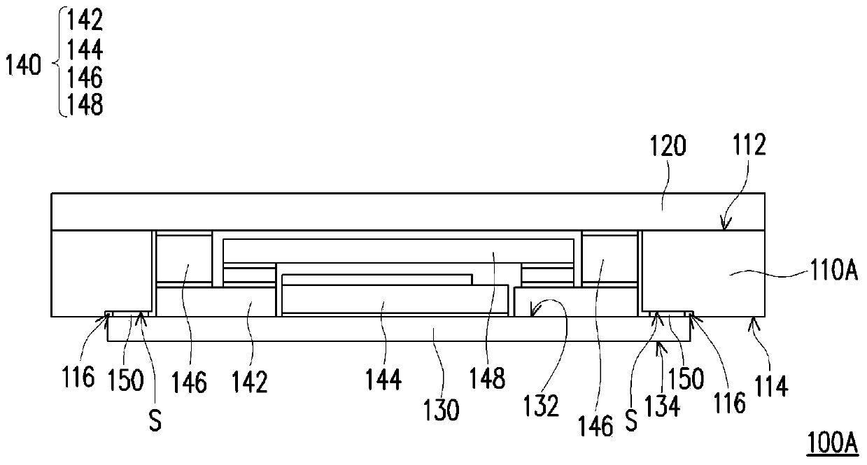
[0038] figure 1 It is a schematic diagram of ...


PUM


Abstract

The invention provides an electronic device. The electronic device comprises a frame body, a display panel, a bottom plate and a fingerprint sensing module, the frame body is provided with a first topsurface and a first bottom surface. The display panel is arranged on the first top surface of the frame body and provides an illumination light beam to a finger so as to reflect a sensing light beam.The bottom plate is arranged on the frame body and is provided with a second top surface and a second bottom surface which are parallel to each other; the fingerprint sensing module is disposed on the second top surface of the bottom plate and receives the sensing light beam.

Description

technical field [0001] The invention relates to an electronic device, in particular to an electronic device with a fingerprint identification function. Background technique [0002] With the development of portable electronic devices (such as smart phones or tablet computers) toward larger screen ratios or full screens. In the process of manufacturing an electronic device including an optical fingerprint sensing module, it is necessary to process the steel plate used to carry the fingerprint sensing module in a special shape, and then process the middle frame of the electronic device, so that the above two components can be used in the subsequent Assemble in process. However, this method will result in that the shape of the steel plate needs to be processed in accordance with the middle frame structure, which will increase the manufacturing cost. Moreover, due to the large number of processing times, the assembly tolerance is increased, resulting in a decline in assembly y...

Claims


Application Information

Patent Timeline
Patent Type & Authority Applications(China)
IPC IPC(8): G06K9/00
CPCG06V40/1318
Inventor 刘彦铭王冠渊林东毅
Owner EGIS TECH
Features
  • R&D
  • Intellectual Property
  • Life Sciences
  • Materials
  • Tech Scout
  • Unparalleled Data Quality
  • Higher Quality Content
  • 60% Fewer Hallucinations
Learn More