Pixel structure and display panel
A pixel structure and pixel technology, applied in the direction of semiconductor devices, electrical components, circuits, etc., can solve the problems that the quality of the display panel needs to be improved, the border of the display area has obvious jaggedness, etc., and achieve the effect of improving the display effect and smoothing the jaggedness
- Summary
- Abstract
- Description
- Claims
- Application Information
AI Technical Summary
Problems solved by technology
Method used
Image


Examples
Embodiment Construction
[0026] In order to make the purpose, technical solutions and advantages of the embodiments of the present invention more clear, various implementation modes of the present invention will be described in detail below in conjunction with the accompanying drawings. However, those of ordinary skill in the art can understand that in each implementation manner of the present invention, many technical details are proposed in order to enable readers to better understand the present invention. However, even without these technical details and various changes and modifications based on the following implementation modes, the technical solution claimed in the present invention can also be realized.
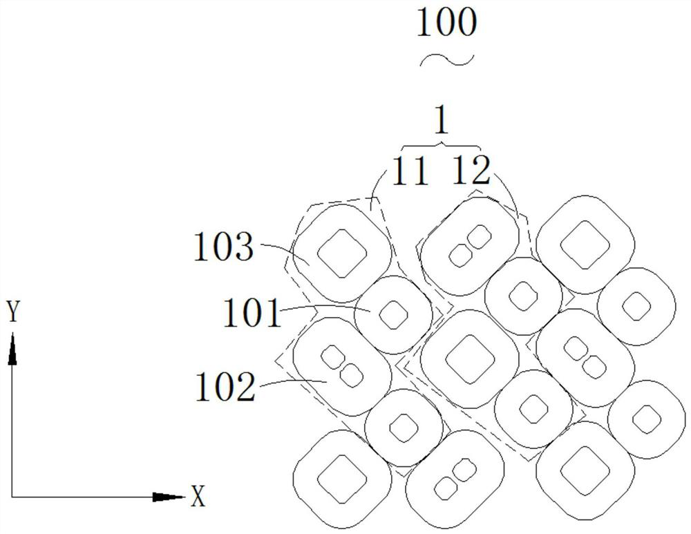
[0027] The first embodiment of the present invention relates to a pixel structure 100, the specific structure is as follows figure 1 and figure 2 shown, including:
[0028] A plurality of repeating units 1 arranged in an array, each repeating unit 1 includes a first pixel group 11 and a s...
PUM
 Abstract
Description
Claims
Application Information