Charge control device for systems with multiple electron beams
一种电子束、电子源的技术,应用在电路、放电管、电气元件等方向,能够解决复杂等问题
- Summary
- Abstract
- Description
- Claims
- Application Information
AI Technical Summary
Problems solved by technology
Method used
Image

Examples
Embodiment Construction
[0037] Although the claimed subject matter will be described in terms of certain embodiments, other embodiments, including embodiments that do not provide all of the advantages and features set forth herein, are also within the scope of the invention. Various structural, logical, process step, and electronic changes may be made without departing from the scope of the present invention. Accordingly, the scope of the present invention is to be defined only with reference to the appended claims.
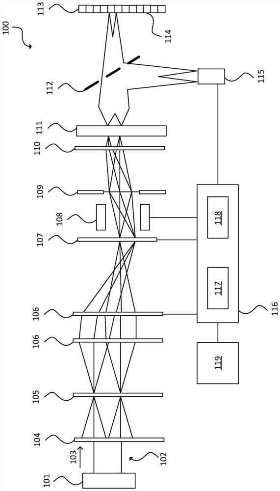
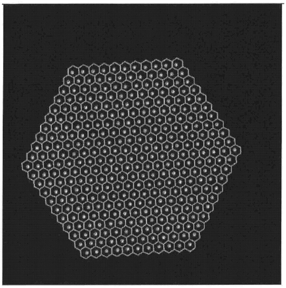
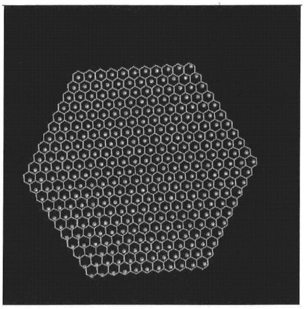
[0038]Scanning Electron Multiple Beam Microscopy (SEMM) can form beam arrays by imaging a point source of electrons on a wafer through an array of microapertures. The array of locations at the wafer from which secondary electrons are emitted is inversely scanned and imaged on a scintillator. The optical image can be relayed and aligned to the fiber array so that the intensity of each fiber element represents the pixel intensity of each secondary beam at any given time. The intensities...
PUM
 Abstract
Description
Claims
Application Information
 - R&D
- Intellectual Property
- Life Sciences
- Materials
- Tech Scout
- Unparalleled Data Quality
- Higher Quality Content
- 60% Fewer Hallucinations
Browse by: Latest US Patents, China's latest patents, Technical Efficacy Thesaurus, Application Domain, Technology Topic, Popular Technical Reports.
© 2025 PatSnap. All rights reserved.Legal|Privacy policy|Modern Slavery Act Transparency Statement|Sitemap|About US| Contact US: help@patsnap.com