Image and light source modulation for a digital display system

light source technology, applied in the field of image processing and modulation system of a digital display system, can solve the problems of reducing magnification, difficult to achieve acceptable visual quality, and changing display characteristics, so as to improve image consistency, enhance color gamut, and improve dynamic range

Active Publication Date: 2007-02-15
SAMSUNG ELECTRONICS CO LTD
View PDF16 Cites 354 Cited by
  • Summary
  • Abstract
  • Description
  • Claims
  • Application Information

AI Technical Summary

Benefits of technology

[0027] The present invention provides an apparatus and method for performing image processing that controls both the image modulator and the light sources to enhance display quality.
[0030] An exemplary Flat Panel Display system has a patterned array of red, green and blue LEDs as the back light and a TFT panel as the image modulator. The 240 LEDs are individually controlled but the resolution of the TFT panel is 1600×1200 pixels. Various filters and diffusion films are used to produce color and brightness as consistent and uniform as possible across the panel. Depending on its position on the panel, each TFT pixel is affected by one or more RGB LED triplets. The Display Output Processing (DOP) for this exemplary system modulates each LED to control its brightness and adjusts the per pixel values for the TFT panel. The resulting display has improved image consistency, enhanced color gamut, and higher dynamic range, and is better able to portray high motion content.

Problems solved by technology

Manufacturing FPDs requires special processing steps and it is often difficult to achieve acceptable visual quality in terms of consistence across the entire area of the display.
Besides being a yield issue for new displays, display characteristics can change over operating conditions and over the lifetime of the display.
Radial distortion includes barrel distortion, where image magnification decreases towards the corners, and pin cushion distortion, where the magnification increases towards the corners.
Lens related distortions including radial distortion can cause image deformation.
Distortion can also result from non-flat screens or the Earth's magnetic field.
Shortening the projection path, often done to thin a rear projection system, also increases distortion.
Each color component of the pixels mapped to the screen display pixels may transfer non uniformly where some pixels end up too bright and others end up not bright enough.
This non-uniformity may be a function of the light path characteristics, the mirrors, the lenses, the lamps or any combination thereof Similarly for LED backlit FPDs, the spacing and positioning of the LEDs may cause non-uniform brightness patterns where the image modulator pixels closer to the LEDs appear brighter than the image modulator pixels further from the LEDs.
However, because of the nature of LCD image modulator pixels, the transitions for modulating light intensities are not purely digital, and are not necessarily linear.
The light sources for a modulator based system may not be able to accurately and uniformly reproduce the intended color gamut, and different modulator pixel positions on the screen may be affected by the light sources differently, causing a display of non-uniform color and brightness.

Method used


Image

  • Image and light source modulation for a digital display system
  • Image and light source modulation for a digital display system
  • Image and light source modulation for a digital display system

Examples


Embodiment Construction

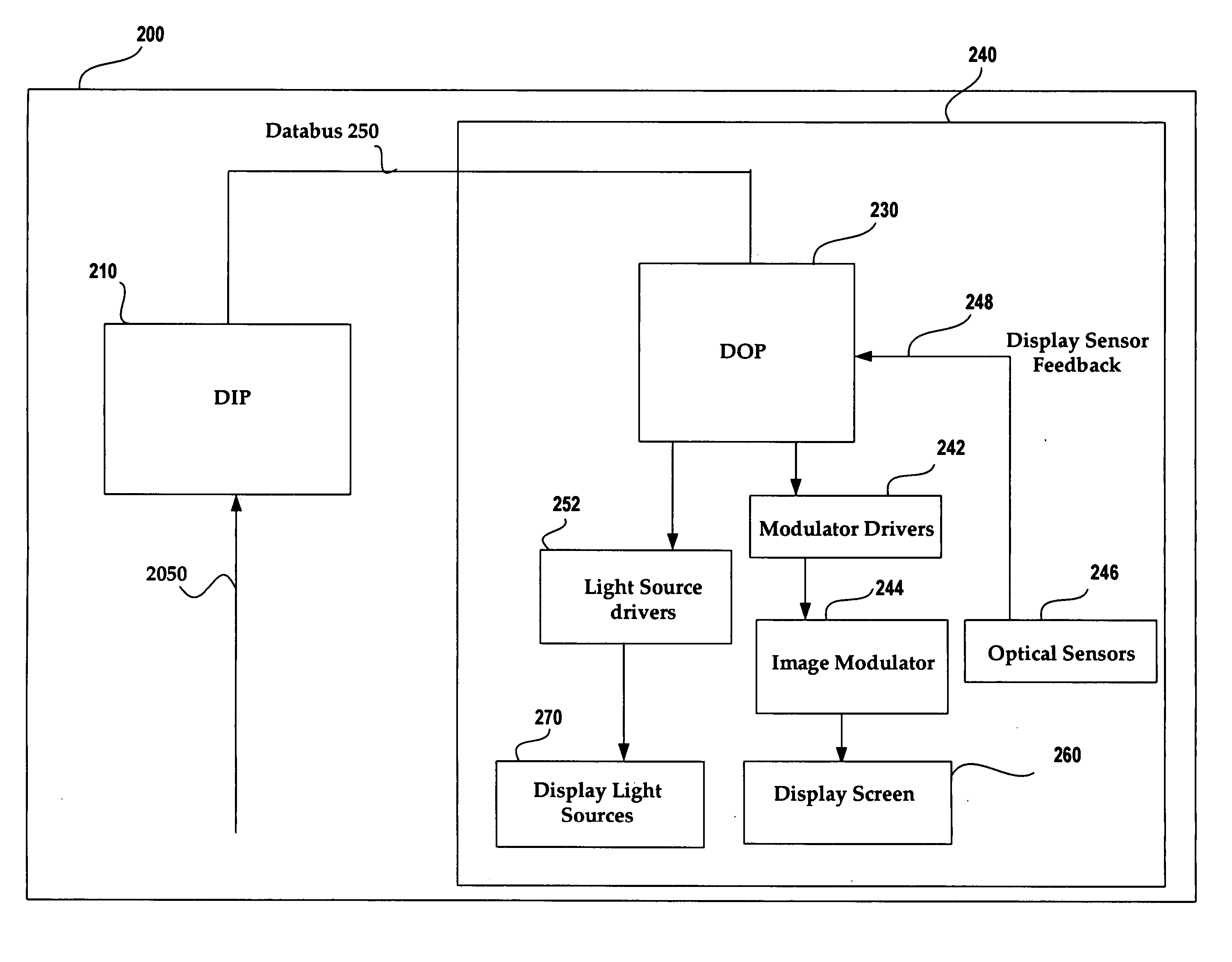
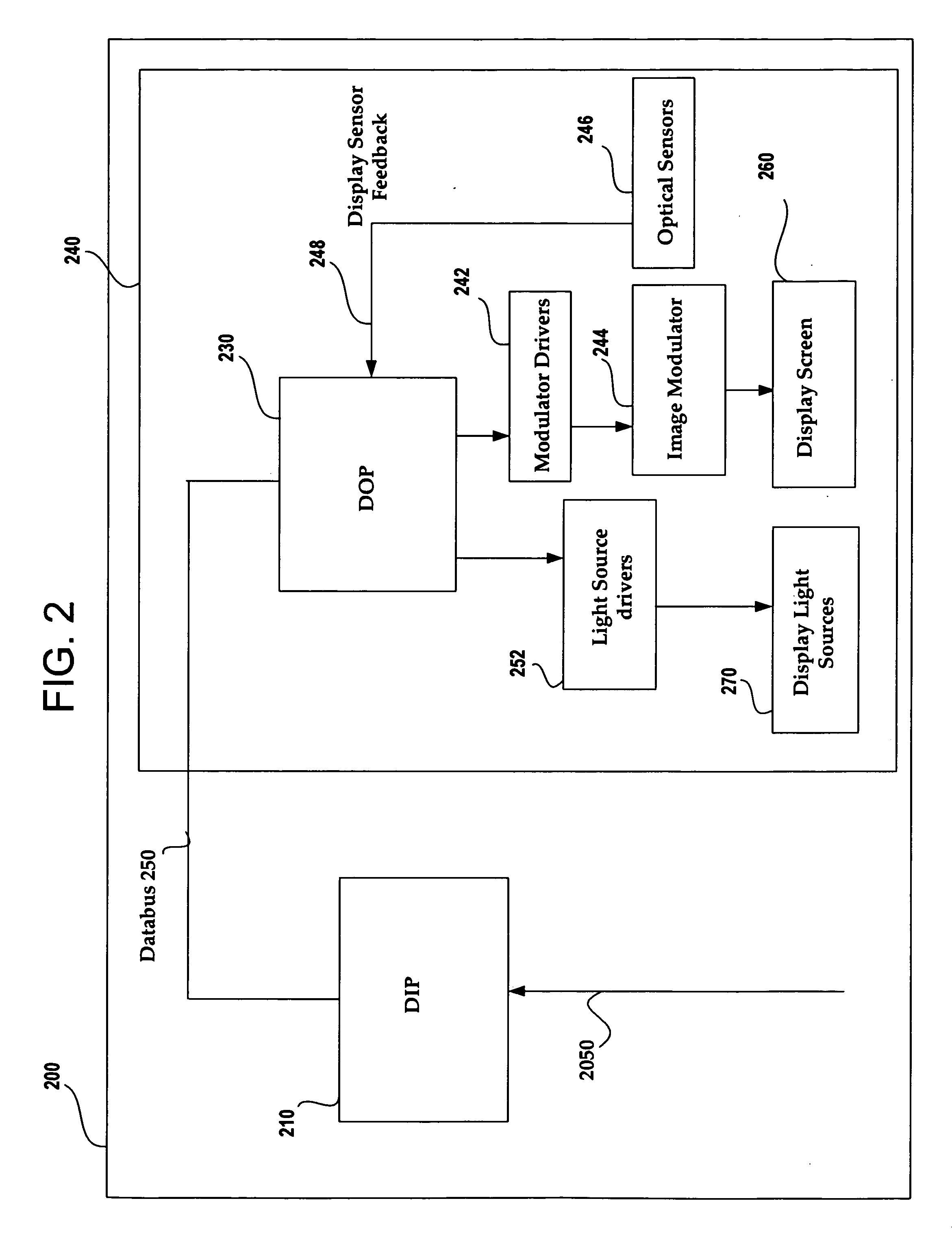
[0041] The present invention provides improvements in electronic image processing technology and an image processing apparatus for use in an image display system. The apparatus includes a display output processing module that controls both a digital image modulator and one or more light sources illuminating the image modulator.

[0042]FIG. 2 shows an image processing system 200 which includes a Display Input Processor (DIP) 210 and a Display System 240 including a Display Output Processor (DOP) 230 with a common databus 250 coupling the DIP 210 and the DOP 230. Display System 240 also includes an image modulator 244 (comparable to FIG. 1 modulators 110 and 130) coupled to a display screen 260 and via modulator drivers 242 to DOP 230. DOP 230 also includes light source drivers 252 coupled to the display light sources 270 and receives display sensor feedback via path 248 from optical sensors 246. DIP 210 preferably receives image data on line 2050 and reconstructs images both spatially...


PUM


Abstract

Image processing enhances display quality by controlling both the image modulator and the light sources to produce the best possible visual images. The image processing system utilizes a combination of user inputs, system configuration, design information, sensor feedback, pixel modulation information, and lighting control information to characterize the display environment on a per pixel basis. This per pixel characterization information is combined with one or more frames of the incoming real time display data. The image processing system processes each incoming pixel and produces a modified corresponding output pixel. Each pixel of each frame is processed accordingly. In addition to producing modified output pixels, the image processing system produces control information for the light sources. The light source control information can control individual lamps, tubes or LEDs, or can control a block or subset of the light sources. The resulting display has improved image consistency, enhanced color gamut, higher dynamic range and is better able to portray high motion content.

Description

[0001] This application is a Continuation-in-Part of U.S. application Ser. No. 11 / 158,476 filed Jun. 20, 2005.BACKGROUND OF THE INVENTION [0002] 1. Field of the Invention [0003] The present invention relates generally to an image processing and modulation system for a digital display system, and more particularly to performing lighting control along with advanced image processing and image modulation to produce high-quality output images. [0004] 2. Discussion of Prior Art [0005] The many types of Flat Panel Display (FPD) technologies include Active Matrix Liquid Crystal Displays (AMLCDs) also referred to as Thin Film Transistor displays (TFTs), silicon Reflective LCDs (si-RLCDs), Liquid Crystal On Silicon (LCOS), ferroelectric displays (FLCs), Field Emission Displays (FEDs), Carbon Nanotube based Nano Emissive Displays (NEDs), ElectroLuminescent Displays (ELDs), Light Emitting Diodes (LEDs), Organic LEDs (OLEDs), Plasma Displays (PDs), Passive matrix Liquid Crystal Displays (LCDs), ...

Claims


Application Information

Patent Timeline
Patent Type & Authority Applications(United States)
IPC IPC(8): G03B21/00
CPCG03B21/00G03B21/2046G09G3/2096G09G3/342G09G3/3433G09G5/363G09G2300/023G09G2320/062G09G2320/106G09G2340/0407G09G2360/142G09G2360/18H04N9/3102H04N9/3155H04N9/3161H04N9/3179H04N9/3194H04N9/3197G03B21/2053G03B21/20G03B21/005
Inventor MARGULIS, NEAL D.
Owner SAMSUNG ELECTRONICS CO LTD
Why Eureka
Try Eureka