A six-layer wiring lcp packaging substrate, manufacturing method and multi-chip system-in-package structure

A technology for encapsulating substrates and substrates, applied in semiconductor/solid-state device manufacturing, semiconductor/solid-state device parts, semiconductor devices, etc., to achieve excellent high-frequency transmission characteristics, reduced use, low moisture absorption and water permeability, and oxygen transmission rate Effect

Active Publication Date: 2022-05-10
SOUTHWEST CHINA RES INST OF ELECTRONICS EQUIP
View PDF17 Cites 0 Cited by
  • Summary
  • Abstract
  • Description
  • Claims
  • Application Information

AI Technical Summary

Problems solved by technology

[0016] The existing disclosed technology has not yet used LCP to realize the technical solution of packaging substrate and system-in-package structure that meets the system-in-package requirements of multi-chip, high airtightness requirements, high electromagnetic shielding, and highly reliable interconnection.

Method used


Image

  • A six-layer wiring lcp packaging substrate, manufacturing method and multi-chip system-in-package structure
  • A six-layer wiring lcp packaging substrate, manufacturing method and multi-chip system-in-package structure
  • A six-layer wiring lcp packaging substrate, manufacturing method and multi-chip system-in-package structure

Examples


Embodiment 1

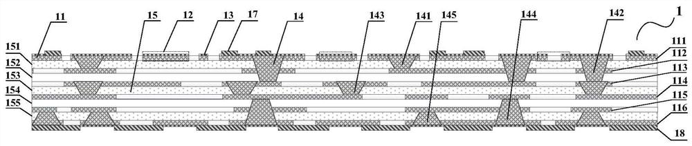
[0077] Such as figure 1 As shown, a six-layer wiring LCP packaging substrate of this embodiment includes:

[0078] 6 layers of patterned metal circuit layers distributed from the surface to the bottom surface, followed by the first layer of patterned metal circuit layer, the second layer of patterned metal circuit layer, the third layer of patterned metal circuit layer, and the fourth layer of patterned metal circuit layer layer, the fifth layer of patterned metal circuit layer and the sixth layer of patterned metal circuit layer; the sixth layer of patterned metal circuit layer is provided with a structure for welding BGA solder balls;

[0079] 5 layers of insulating dielectric layers between adjacent patterned metal circuit layers;

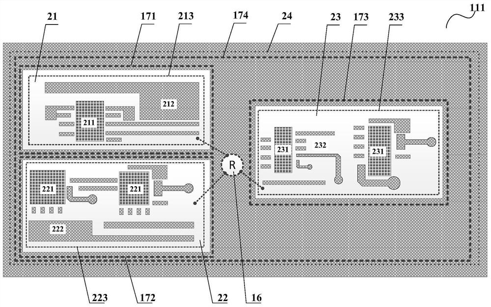
[0080] Multiple chip mounting areas located on the first patterned metal circuit layer;

[0081] A plurality of blind holes located between the patterned metal circuit layer and the insulating medium layer are used to realize the interconnecti...

Embodiment 2

[0100] Such as image 3 As shown, this embodiment provides a method for manufacturing the six-layer wiring LCP packaging substrate 1 as described in Embodiment 1, including the following steps:

[0101] S1, such as Figure 5a As shown, blind holes are laser drilled on the second double-sided copper-clad LCP substrate 153 to form third-type blind holes 143 that penetrate and connect the third patterned metal circuit layer 113 and the fourth layer patterned metal circuit layer 114, Blind hole depth-to-diameter ratio ≤ 1;

[0102] S2, such as Figure 5b As shown, the metallization of blind holes forms the third type of blind holes 143 filled with solid electroplated copper; The electroplating copper process is realized. After hole filling electroplating, the copper plating layer on the surface is thinned to form a third type of blind hole 143 filled with solid electroplated copper;

[0103] S3, such as Figure 5c As shown, the third patterned metal circuit layer 113 and the ...

Embodiment 3

[0113] As shown in FIG. 5, based on the LCP packaging substrate described in Embodiment 1-2, this embodiment provides a multi-chip system-in-package structure 61, including: the LCP packaging substrate 1 described in Embodiment 1-2, and BGA solder ball 2, chip 3, metal frame 5 and metal cover 6;

[0114] The BGA solder balls 2 are soldered to the bottom surface of the LCP packaging substrate 1, and serve as the external secondary cascade I / O interface of the multi-chip system-in-package structure 61;

[0115] Metal partitions 51 are distributed in the metal enclosure 5; the metal enclosure 5 and the metal partitions 51 are welded to the upper surface of the LCP packaging substrate 1, and the metal cover 6 is welded to the metal enclosure 5 and the metal partitions 51, between the LCP packaging substrate 1 and the metal cover plate 6, a plurality of cavity structures 7 with airtight sealing performance and electromagnetic shielding performance are formed through the metal surro...


PUM


Abstract

The invention discloses a six-layer wiring LCP packaging substrate, a manufacturing method and a multi-chip system-level packaging structure. The LCP packaging substrate includes: 6 layers of patterned metal circuit layers distributed from the surface to the bottom surface; 5 layers of insulating dielectric layers between the circuit layers; multiple chip mounting areas located on the first patterned metal circuit layer; multiple blind holes located between the patterned metal circuit layer and the insulating dielectric layer, used to realize 6 Any layer interconnection requirements in the layer patterned metal line layer. The invention realizes an LCP packaging substrate with an airtight packaging structure that can meet the system-level packaging requirements of multiple chips, high airtightness, high electromagnetic shielding, and high reliability interconnection.

Description

technical field [0001] The invention relates to the technical field of integrated circuits and chip packaging, in particular to a six-layer wiring LCP packaging substrate, a manufacturing method and a multi-chip system-level packaging structure, which are used for high-reliability system-level applications for high-frequency applications such as radio frequency, microwave, and millimeter wave. encapsulation. Background technique [0002] With the advancement of semiconductor and integrated circuit technology, the requirements for system integration have been further improved. The current design and manufacture of electronic circuits are moving towards smaller sizes and higher integration densities. Considerable work is carried out in the field of multi-chip packaging. In the advanced packaging form, multiple radio frequency (RF) chips, digital integrated circuit (IC) chips, micro-chip components, etc. are assembled on the packaging substrate through SIP technology, and then ...

Claims


Application Information

Patent Timeline
Patent Type & Authority Patents(China)
IPC IPC(8): H01L23/538H01L23/498H01L23/552H01L21/48H01L21/768
CPCH01L23/49894H01L23/49838H01L23/5386H01L23/552H01L23/49816H01L21/4846H01L21/4853H01L21/76895H01L2224/48091H01L2224/48227H01L2924/15311H01L2924/00014
Inventor 徐诺心戴广乾边方胜易明生廖翱卢军林玉敏赵鸣霄曾策杜顺勇
Owner SOUTHWEST CHINA RES INST OF ELECTRONICS EQUIP
Why Eureka
Try Eureka