Airtight high-thermal-conductivity LCP packaging substrate and multi-chip system-in-package structure

A packaging substrate, high thermal conductivity technology, applied in the direction of electrical components, semiconductor devices, semiconductor/solid-state device components, etc., to achieve the effects of simple packaging, good compatibility, and high assembly efficiency

Pending Publication Date: 2021-02-09
SOUTHWEST CHINA RES INST OF ELECTRONICS EQUIP
View PDF16 Cites 0 Cited by
  • Summary
  • Abstract
  • Description
  • Claims
  • Application Information

AI Technical Summary

Problems solved by technology

[0016] The existing disclosed technology has not yet used LCP to realize the technical solution of packaging substrate and system-in-package structure that meets the system-in-package requirements of multi-chip, high airtightness requirements, high electromagnetic shielding, high thermal conductivity requirements, and high reliability interconnection.

Method used


Image

  • Airtight high-thermal-conductivity LCP packaging substrate and multi-chip system-in-package structure
  • Airtight high-thermal-conductivity LCP packaging substrate and multi-chip system-in-package structure
  • Airtight high-thermal-conductivity LCP packaging substrate and multi-chip system-in-package structure

Examples


Embodiment 1

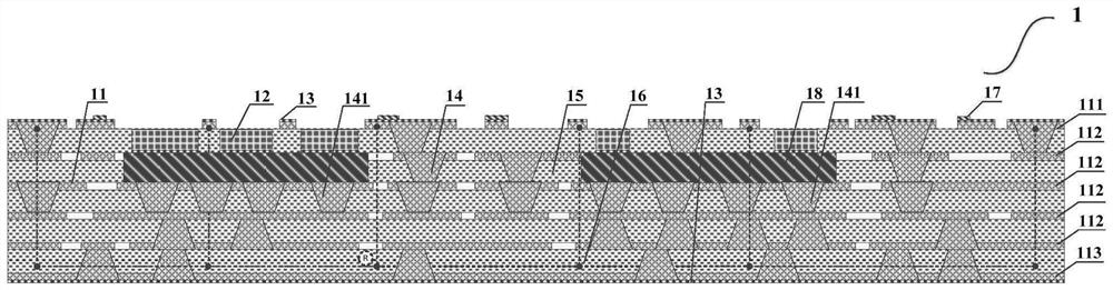
[0051] Such as figure 1 As shown, a kind of airtight high thermal conductivity LCP package substrate of the present embodiment comprises:

[0052] There are n layers of patterned metal circuit layers distributed from the surface to the bottom surface. On at least one edge of the outermost edge of the first layer of patterned metal circuit layer on the surface, solder for external secondary cascaded I / O welding of the LCP packaging substrate is distributed. disk or graphics;

[0053] N-1 layers of insulating dielectric layers located between adjacent patterned metal circuit layers;

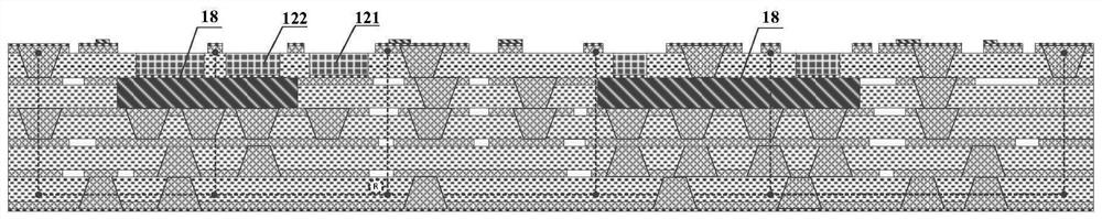
[0054] A plurality of blind grooves of the first patterned metal circuit layer with openings facing the surface in the insulating medium layer between the first patterned metal circuit layer and the second layer patterned metal circuit layer; the blind grooves include Ordinary chip mounting blind slots and high-power chip mounting blind slots;

[0055] A metal block located in the insulating med...

Embodiment 2

[0074] Such as Figure 5 As shown, based on the LCP packaging substrate described in Embodiment 1, this embodiment provides a multi-chip system-in-package structure 2, including: the LCP packaging substrate 1 as described in Embodiment 1, and a chip 3, and a metal frame 5 and metal cover plate 6;

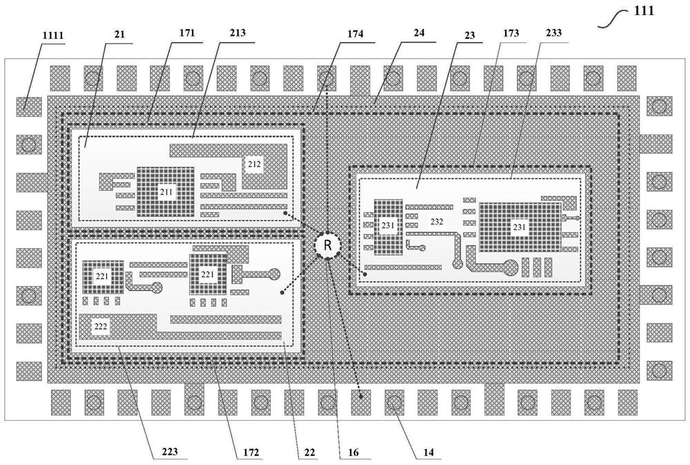
[0075] The multi-chip system-in-package structure 2 is fixed on the PCB mother board by means of conductive adhesive bonding or welding, and the pads or patterns 1111 for external secondary cascading I / O welding on the LCP packaging substrate 1 are used. As the external secondary cascade I / O interface of the multi-chip system-in-package structure 61;

[0076] Metal ribs 51 are distributed in the metal surrounding frame 5; the metal surrounding frame 5 and the metal ribs 51 are welded on the upper surface of the LCP package substrate 1 and make the external secondary cascaded I / O welding pads or Figure 1111 is outside the metal frame 5, and the metal cover plate 6 is welded on the ...


PUM


Abstract

The invention discloses an airtight high-thermal-conductivity LCP packaging substrate and a multi-chip system-in-package structure, and the LCP packaging substrate comprises n graphical metal circuitlayers which are distributed from the surface to the bottom surface, wherein at least one edge of the outermost periphery of the first graphical metal circuit layer on the surface is provided with pads or patterns for external secondary cascade I / O welding of the LCP packaging substrate; n-1 insulating dielectric layers which are positioned between the adjacent graphical metal circuit layers; a plurality of blind grooves which are positioned in the insulating medium layer between the first graphical metal circuit layer and the second graphical metal circuit layer, wherein openings of the blindgrooves face the first graphical metal circuit layer on the surface; a metal block which is positioned in the insulating dielectric layer and is connected with the bottom of the high-power chip mounting blind groove; and a plurality of blind holes which penetrate through and are connected with the adjacent graphical metal circuit layers. The LCP package substrate can meet the system-in-package requirements of multiple chips, high airtightness requirements, high electromagnetic shielding, high thermal conductivity requirements and high reliability interconnection.

Description

technical field [0001] The invention relates to the technical field of integrated circuit and chip packaging, in particular to an airtight high thermal conductivity LCP packaging substrate and a multi-chip system-in-package structure, which are used for high-reliability system-in-package for high-frequency applications such as radio frequency, microwave, and millimeter wave. Background technique [0002] With the advancement of semiconductor and integrated circuit technology, the requirements for system integration have been further improved. The current design and manufacture of electronic circuits are moving towards smaller sizes and higher integration densities. Considerable work is carried out in the field of multi-chip packaging. In the advanced packaging form, multiple radio frequency (RF) chips, digital integrated circuit (IC) chips, micro-chip components, etc. are assembled on the packaging substrate through SIP technology, and then integrated into a package. This mu...

Claims


Application Information

Patent Timeline
IPC IPC(8): H01L23/538H01L23/367H01L23/373H01L23/498H01L23/552H05K1/09
CPCH01L23/49894H01L23/49838H01L23/5386H01L23/552H01L23/367H01L23/3736H01L23/49816H05K1/09H01L2224/48091H01L2924/00014
Inventor 戴广乾曾策易明生廖翱谢国平林玉敏笪余生潘玉华向伟玮徐榕青
Owner SOUTHWEST CHINA RES INST OF ELECTRONICS EQUIP
Why Eureka
Try Eureka