Airtight high-thermal-conductivity LCP packaging substrate, manufacturing method and multi-chip system-in-package structure

A packaging substrate, high thermal conductivity technology, used in semiconductor/solid-state device manufacturing, electrical components, semiconductor devices, etc., to meet the needs of heat dissipation, high electromagnetic shielding, and high assembly efficiency.

Active Publication Date: 2021-02-09
SOUTHWEST CHINA RES INST OF ELECTRONICS EQUIP
View PDF16 Cites 0 Cited by
  • Summary
  • Abstract
  • Description
  • Claims
  • Application Information

AI Technical Summary

Problems solved by technology

[0016] The existing disclosed technology has not yet used LCP to realize the technical solution of packaging substrate and system-in-package structure that meets the system-in-package requirements of multi-chip, high airtightness requirements, high electromagnetic shielding, and highly reliable interconnection.

Method used


Image

  • Airtight high-thermal-conductivity LCP packaging substrate, manufacturing method and multi-chip system-in-package structure
  • Airtight high-thermal-conductivity LCP packaging substrate, manufacturing method and multi-chip system-in-package structure
  • Airtight high-thermal-conductivity LCP packaging substrate, manufacturing method and multi-chip system-in-package structure

Examples


Embodiment 1

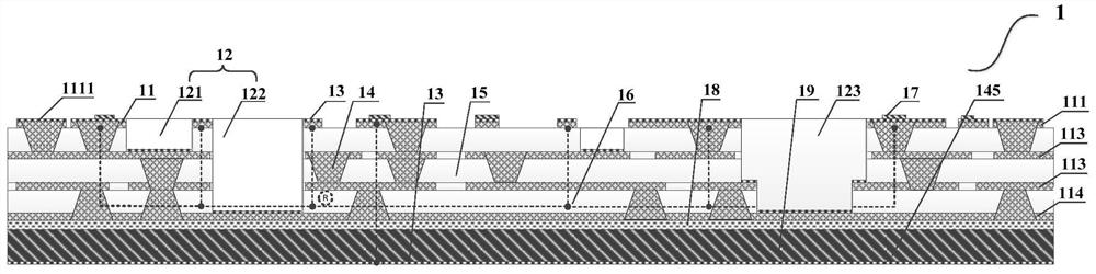
[0058] like figure 1 As shown, a kind of airtight high thermal conductivity LCP packaging substrate of this embodiment includes: any layer of LCP interconnects a multi-layer substrate, an adhesive layer and a metal back plate; the metal back plate is bonded to the LCP through an adhesive layer Arbitrary layers interconnect the bottom surface of multilayer substrates;

[0059] The LCP arbitrary layer interconnection multilayer substrate includes: n layers of patterned metal circuit layers, on at least one edge of the outermost periphery of the first layer of patterned metal circuit layers on the surface, the external secondary cascade I of the LCP packaging substrate is distributed. / O welding pads or patterns; n-1 layers of insulating dielectric layers between adjacent patterned metal circuit layers; a plurality of blind holes that are located in the insulating dielectric layer and open toward the first layer of patterned metal circuit layers Groove; a plurality of blind hole...

Embodiment 2

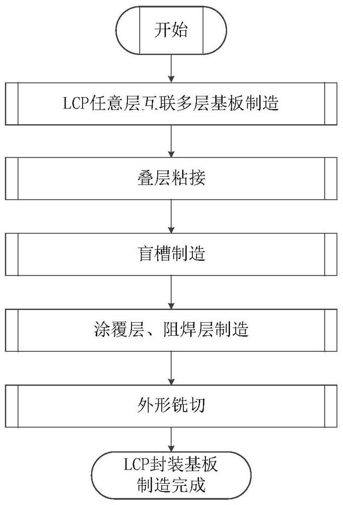
[0077] Such as image 3 As shown, this embodiment provides a method for manufacturing the airtight and high thermal conductivity LCP packaging substrate 1 as described in Embodiment 1, including the following steps:

[0078] S1, such as Figure 4a As shown, the HDI lamination process is used to manufacture LCP arbitrary layer interconnection multi-layer substrates, and the position of the blind slot is preset. The patterned metal circuit layer corresponding to the preset blind slot position does not have metal lines;

[0079] S2, take the adhesive layer 18 and the metal backplane 19, and then interconnect the multilayer substrate, the adhesive layer, and the metal backplane according to the sequence of any layer of the LCP from top to bottom, according to Figure 4b stack as shown and then bonded as Figure 4c the structure shown;

[0080] S3, such as Figure 4d As shown, use laser processing means to carry out blind slot slotting at the preset blind slot position to form ...

Embodiment 3

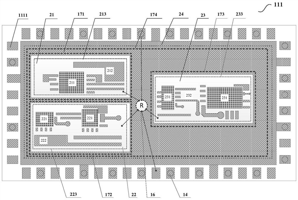
[0085] Such as Figure 5 As shown, based on the LCP packaging substrate described in Embodiment 1-2, this embodiment provides a multi-chip system-in-package structure 2, including: the LCP packaging substrate 1 as described in Embodiment 1-2, and chips 3, Metal enclosure 5 and metal cover plate 6;

[0086] The multi-chip system-in-package structure 2 is fixed on the PCB mother board by means of conductive adhesive bonding or welding, and the pads or patterns 1111 for external secondary cascading I / O welding on the LCP packaging substrate 1 are used. As the external secondary cascade I / O interface of the multi-chip system-in-package structure 2;

[0087] Metal ribs 51 are distributed in the metal surrounding frame 5; the metal surrounding frame 5 and the metal ribs 51 are welded on the upper surface of the LCP package substrate 1 and make the external secondary cascaded I / O welding pads or The figure 1111 is outside the metal frame 5, and the metal cover plate 6 is welded on ...


PUM


Abstract

The invention discloses an airtight high-thermal-conductivity LCP packaging substrate, a manufacturing method and a multi-chip system-in-package structure. The LCP packaging substrate comprises an LCParbitrary layer interconnection multilayer substrate, a bonding layer and a metal back plate. The metal back plate is adhered to the bottom surface of the LCP arbitrary layer interconnection multilayer substrate through the bonding layer; the LCP arbitrary layer interconnection multilayer substrate comprises n graphical metal circuit layers, wherein bonding pads or graphs for external secondary cascade I/O welding of the LCP packaging substrate are distributed on at least one edge of the outermost periphery of the first graphical metal circuit layer on the surface; n-1 insulating dielectric layers which are positioned between the adjacent graphical metal circuit layers; a plurality of blind grooves which are located in the insulating dielectric layer, wherein openings of the blind groovesface the first graphical metal circuit layer; and a plurality of blind holes which penetrate through and are connected with the adjacent graphical metal circuit layers. The LCP packaging substrate ofthe airtight packaging structure can meet the system-level packaging requirements of multiple chips, high airtight requirements, high electromagnetic shielding and high reliable interconnection.

Description

technical field [0001] The invention relates to the technical field of integrated circuits and chip packaging, in particular to an airtight high thermal conductivity LCP packaging substrate, a manufacturing method and a multi-chip system-level packaging structure, which are used for high-reliability systems for high-frequency applications such as radio frequency, microwave, and millimeter wave level packaging. Background technique [0002] With the advancement of semiconductor and integrated circuit technology, the requirements for system integration have been further improved. The current design and manufacture of electronic circuits are moving towards smaller sizes and higher integration densities. Considerable work is carried out in the field of multi-chip packaging. In the advanced packaging form, multiple radio frequency (RF) chips, digital integrated circuit (IC) chips, micro-chip components, etc. are assembled on the packaging substrate through SIP technology, and the...

Claims


Application Information

Patent Timeline
Patent Type & Authority Applications(China)
IPC IPC(8): H01L23/538H01L23/498H01L23/367H01L23/373H01L23/552H05K1/09H01L21/48H01L21/768
CPCH01L23/49894H01L23/49838H01L23/5386H01L23/552H01L23/3672H01L23/3736H01L23/49816H05K1/09H01L21/4846H01L21/4853H01L21/76895
Inventor 戴广乾曾策边方胜徐诺心廖翱赵鸣霄舒攀林谢国平张德富潘玉华
Owner SOUTHWEST CHINA RES INST OF ELECTRONICS EQUIP
Why Eureka
Try Eureka