

A protective semiconductor device
A technology of semiconductors and devices, applied in the field of protective semiconductor devices, can solve problems such as device failure, failure to advance or delay control work, and unsuitability
- Summary
- Abstract
- Description
- Claims
- Application Information
AI Technical Summary
Problems solved by technology
Method used
Image

Examples
Embodiment Construction
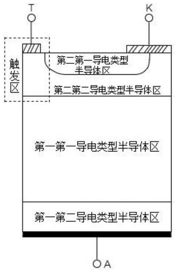
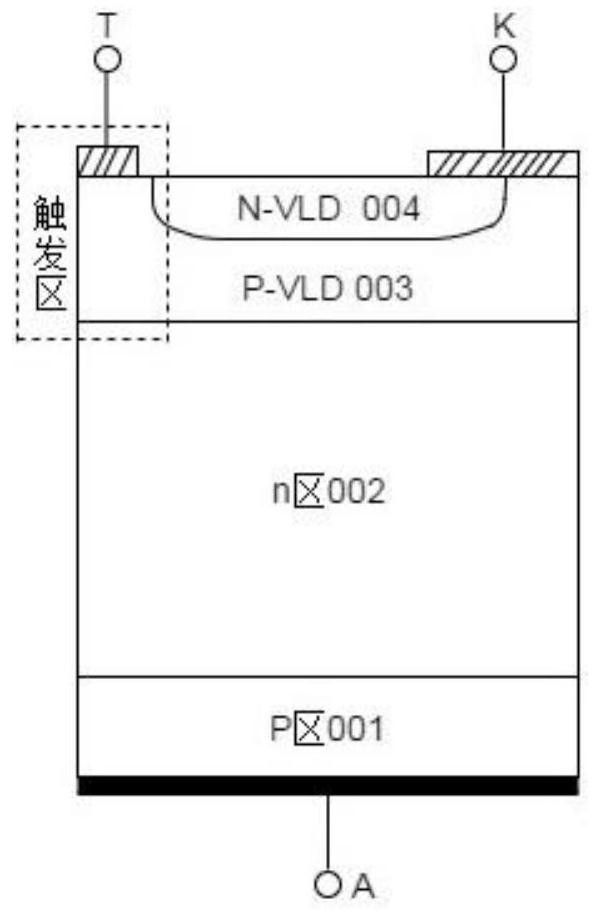
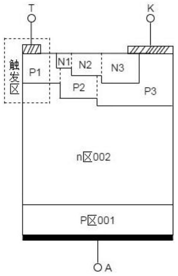
[0034] The technical solution of the present disclosure will be described in detail below in conjunction with the accompanying drawings. In the description of the present application, it should be understood that the terms "first", "second", "third" and "fourth" are used for descriptive purposes only, and should not be understood as indicating or implying relative importance or implicitly The number of technical features indicated is used only to distinguish the different components. In the description of this application, the first conductivity type includes N-type and P-type, and the second conductivity type also includes N-type and P-type. When the first conductivity type is N-type, the second conductivity type is P-type; When the first conductivity type is P-type, the second conductivity type is N-type.
[0035] Additionally, the terms "upper", "lower", "front", "rear", "left", "right", "top", "bottom", "sidewall", "vertical", "horizontal", etc. indicate The orientation ...
PUM
 Abstract
Description
Claims
Application Information