Metal conductive film, manufacturing method, touch panel and electronic product

A technology of metal conduction and manufacturing method, which is applied in the direction of cable/conductor manufacturing, conductive pattern formation, conductive layer on insulating carrier, etc. It can solve the problems of unfavorable large-size conductive film production and the inability of the machine to be directly integrally formed.

Pending Publication Date: 2021-07-30
ANHUI JINGZHUO OPTICAL DISPLAY TECH CO LTD
View PDF0 Cites 0 Cited by
  • Summary
  • Abstract
  • Description
  • Claims
  • Application Information

AI Technical Summary

Problems solved by technology

At present, the technology of using metal grid to make transparent conductive film with a size below 600mm*600mm is very mature, but limited by the existing equipment conditions, it is impossible to prepare an integrated metal grid transparent conductive film with a size above 600mm*600mm , that is, for large-sized transparent conductive films, existing machines cannot directly form one piece, which is not conducive to the production of large-sized conductive films

Method used


Image

  • Metal conductive film, manufacturing method, touch panel and electronic product
  • Metal conductive film, manufacturing method, touch panel and electronic product
  • Metal conductive film, manufacturing method, touch panel and electronic product

Examples


Embodiment

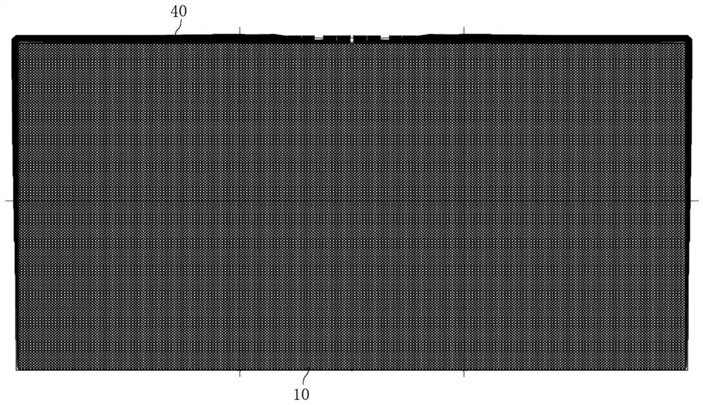
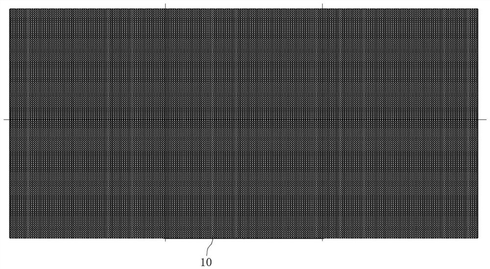
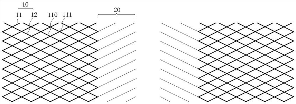
[0042] refer to Figure 1-6 , a metal grid conductive film, comprising at least two traces in the same form and located in the same plane, and the splices are superimposed to form a continuous metal grid layer 10, wherein the base of the metal grid layer is formed along the original The split part 20 for splicing is extended by trace extension, and the split part is superimposed and arranged to form a patchwork 30 for realizing continuous conduction between the metal grid layers to be spliced. When splicing, multiple metal grid layers can be spliced ​​along the same plane. Specifically, the split parts of the metal grid layers to be spliced ​​are stacked together to form a continuous conductive seam, so as to ensure that the grid A continuous conduction whole is formed between the grid layer and the grid layer, so as to solve the problem that the existing equipment cannot integrally form a large-sized metal conductive film.

[0043] As a preferred technical solution of the pr...


PUM

PropertyMeasurementUnit
pore sizeaaaaaaaaaa

Abstract

The invention provides a metal grid conductive film which comprises at least two metal grid layers which are consistent in wiring form and located in the same plane, the splicing positions of the metal grid layers are arranged in an overlapped mode to form a continuous trend, and a splitting part used for splicing is formed on the base portion of each metal grid layer along the extension of the original wiring. The splitting part is arranged in an overlapped mode to form an abutted seam used for achieving continuous conduction between the metal grid layers to be spliced, and the abutted seam comprises an irregular area which is formed by the splitting part and the base portion in an overlapped mode and is different from an original metal grid layer pattern. The invention further discloses a manufacturing method of the metal grid conductive film, a touch panel and an electronic product. When the large-size metal conductive film is prepared, a plurality of metal grid layers can be used for splicing, and particularly, the split parts of the metal grid layers to be spliced are overlapped together to form a continuously-conducted splicing seam, so that a continuously-conducted whole is formed between the grid layers, and the splicing quality is ensured.

Description

technical field [0001] The invention relates to the technical field of metal conductive films, in particular to a metal conductive film, a manufacturing method, a touch panel and electronic products. Background technique [0002] Transparent conductive film is a thin film with high transparency and conductive properties in the visible light range. It is mainly used in optoelectronic devices such as transparent electrodes of liquid crystal displays, touch screens, and transparent electrodes of thin-film solar cells. At present, the technology of using metal grid to make transparent conductive film with a size below 600mm*600mm is very mature, but limited by the existing equipment conditions, it is impossible to prepare an integrated metal grid transparent conductive film with a size above 600mm*600mm , that is, for large-sized transparent conductive films, existing machines cannot directly form one piece, which is not conducive to the production of large-sized conductive film...

Claims


Application Information

Patent Timeline
Patent Type & Authority Applications(China)
IPC IPC(8): H05K3/12H01B13/00H01B5/14G06F3/041
CPCG06F3/0412G06F2203/04103H01B5/14H01B13/00H05K3/12
Inventor 蔡荣陈禄禄陈庆中钟文婷
Owner ANHUI JINGZHUO OPTICAL DISPLAY TECH CO LTD
Why Eureka
Try Eureka