Unlock instant, AI-driven research and patent intelligence for your innovation.

Pixel array substrate

A technology of pixel array substrate and pixel row, which is applied in optics, instruments, electrical components, etc., and can solve problems such as impact and abnormal display

Pending Publication Date: 2022-02-18
AU OPTRONICS CORP
View PDF0 Cites 0 Cited by
  • Summary
  • Abstract
  • Description
  • Claims
  • Application Information

AI Technical Summary

Problems solved by technology

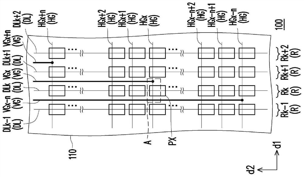
However, the gate turn-on pulse signal of the transfer line will affect the potential of other pixel structures that are still being charged, resulting in abnormal display (for example: oblique bright lines)
Therefore, how to improve the problem of abnormal display is one of the challenges faced by current ultra-narrow bezel display devices.

Method used


Image

  • Pixel array substrate
  • Pixel array substrate
  • Pixel array substrate

Examples


Embodiment Construction

[0095] Reference will now be made in detail to the exemplary embodiments of the present invention, examples of which are illustrated in the accompanying drawings. Wherever possible, the same reference numbers will be used in the drawings and description to refer to the same or like parts.

[0096] It will be understood that when an element such as a layer, film, region, or substrate is referred to as being "on" or "connected to" another element, it can be directly on or connected to the other element, or Intermediate elements may also be present. In contrast, when an element is referred to as being "directly on" or "directly connected to" another element, there are no intervening elements present. As used herein, "connected" may refer to physical and / or electrical connection. Furthermore, "electrically connected" or "coupled" may mean that other elements exist between two elements.

[0097] As used herein, "about," "approximately," or "substantially" includes stated values ...


PUM


Abstract

A pixel array substrate comprises a plurality of pixel structures. Each pixel structure comprises a first common electrode, a thin film transistor, a conductive pattern, a first insulating layer, a color filter pattern, a second insulating layer and a pixel electrode. The conductive pattern is electrically connected to the thin film transistor. The first portion of the conductive pattern is disposed on the first common electrode. The first insulating layer is disposed on the conductive pattern. The color filter pattern is disposed on the first insulating layer. The second insulating layer is disposed on the color filter pattern. The pixel electrode is arranged on the second insulating layer. In a top view of the pixel array substrate, the first portion of the conductive pattern covers all edges of the first common electrode located in the opening of the color filter pattern.

Description

technical field [0001] The invention relates to a pixel array substrate. Background technique [0002] With the development of display technology, people's demand for display devices is no longer satisfied with optical properties such as high resolution, high contrast, and wide viewing angle. People also expect the display device to have an elegant appearance. For example, people expect display devices to have narrow bezels, or even no bezels. [0003] Generally speaking, a display device includes a plurality of pixel structures disposed in the display area, a data driving circuit disposed below the display area, and gate driving circuits disposed on the left, right, or both sides of the display area. In order to reduce the width of the left and right sides of the frame of the display device, both the gate driving circuit and the data driving circuit can be arranged on the lower side of the display area. When the gate driving circuit is disposed on the lower side of the di...

Claims


Application Information

Patent Timeline
Patent Type & Authority Applications(China)
IPC IPC(8): H01L27/12
CPCH01L27/1214H01L27/124G02F2201/40G02F1/136222G02F1/133707G02F1/134309G02F1/136213G02F1/136227G02F1/13452G02F2201/501G02F1/1362G02F2201/121G09G2300/0465G09G2310/0267G09G2320/0209G09G2320/0219H01L27/1218H01L27/1248
Inventor 巫岳锜余悌魁廖淑雯
Owner AU OPTRONICS CORP