Insulating grid type semiconductor device

An insulated gate, semiconductor technology, used in semiconductor devices, electrical components, circuits, etc., can solve problems such as cost increase, and achieve the effect of suppressing sharp rise and suppressing voltage

Inactive Publication Date: 2007-05-23
KK TOSHIBA
View PDF5 Cites 0 Cited by
  • Summary
  • Abstract
  • Description
  • Claims
  • Application Information

AI Technical Summary

Problems solved by technology

Thus, suppression of switching noise comes at an increased cost
[0005] As mentioned above, in the past, the speed was increased by reducing the capacitance between the gate and the drain, but it was necessary to suppress the switching noise, so there was a problem that soft switching was required and an external circuit such as a filter circuit was required.

Method used


Image

  • Insulating grid type semiconductor device
  • Insulating grid type semiconductor device
  • Insulating grid type semiconductor device

Examples


no. 1 Embodiment approach

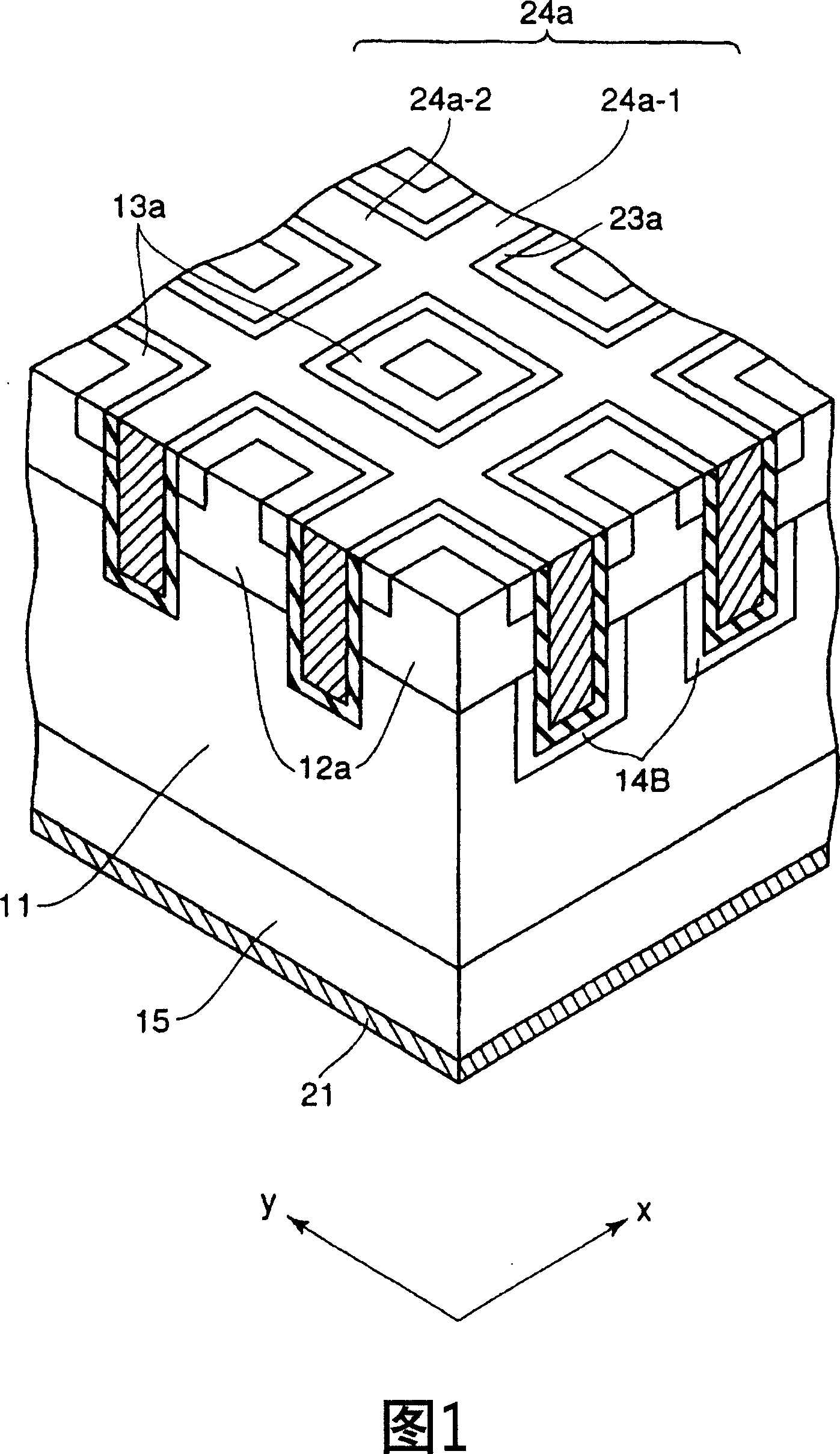
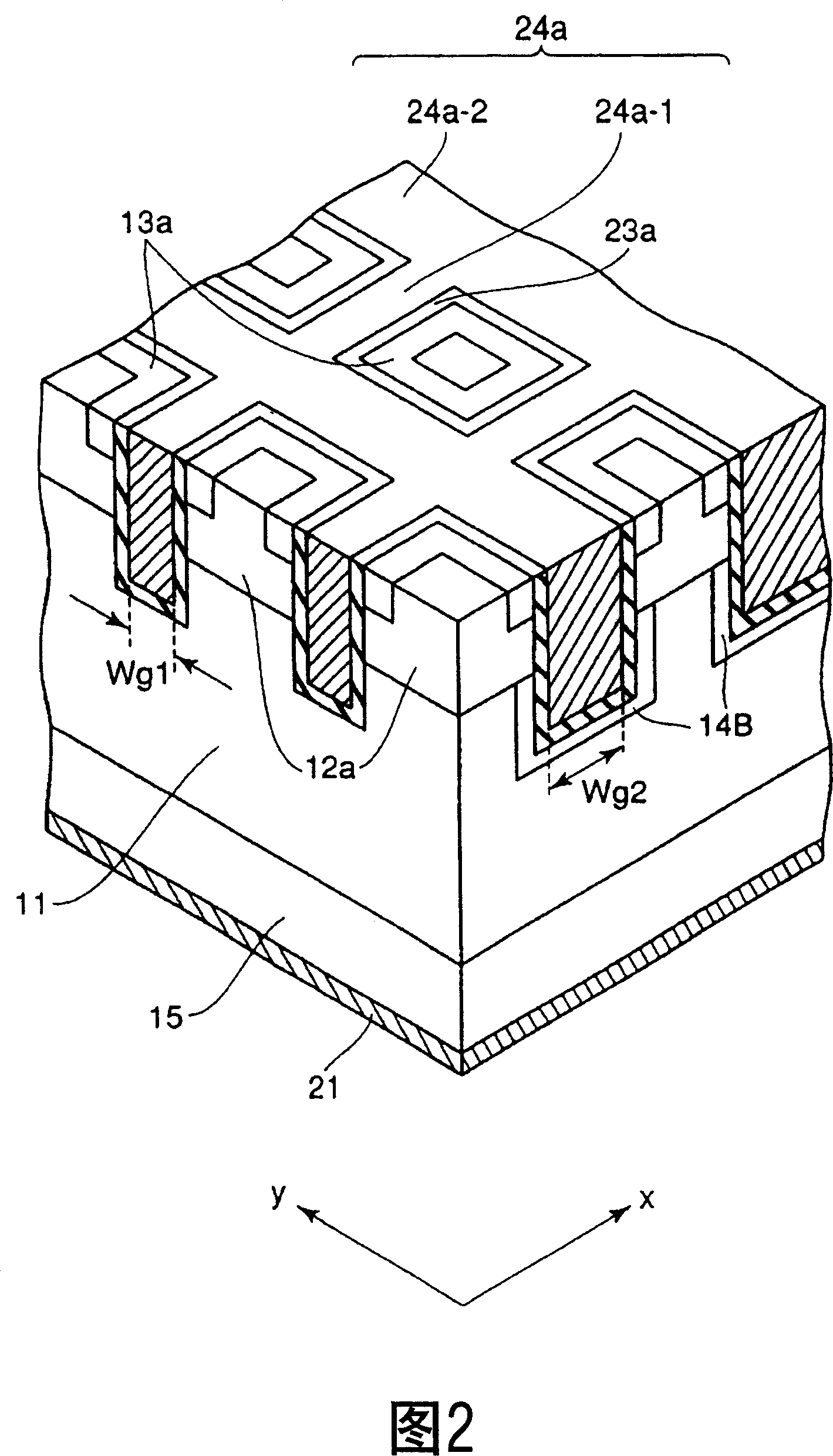
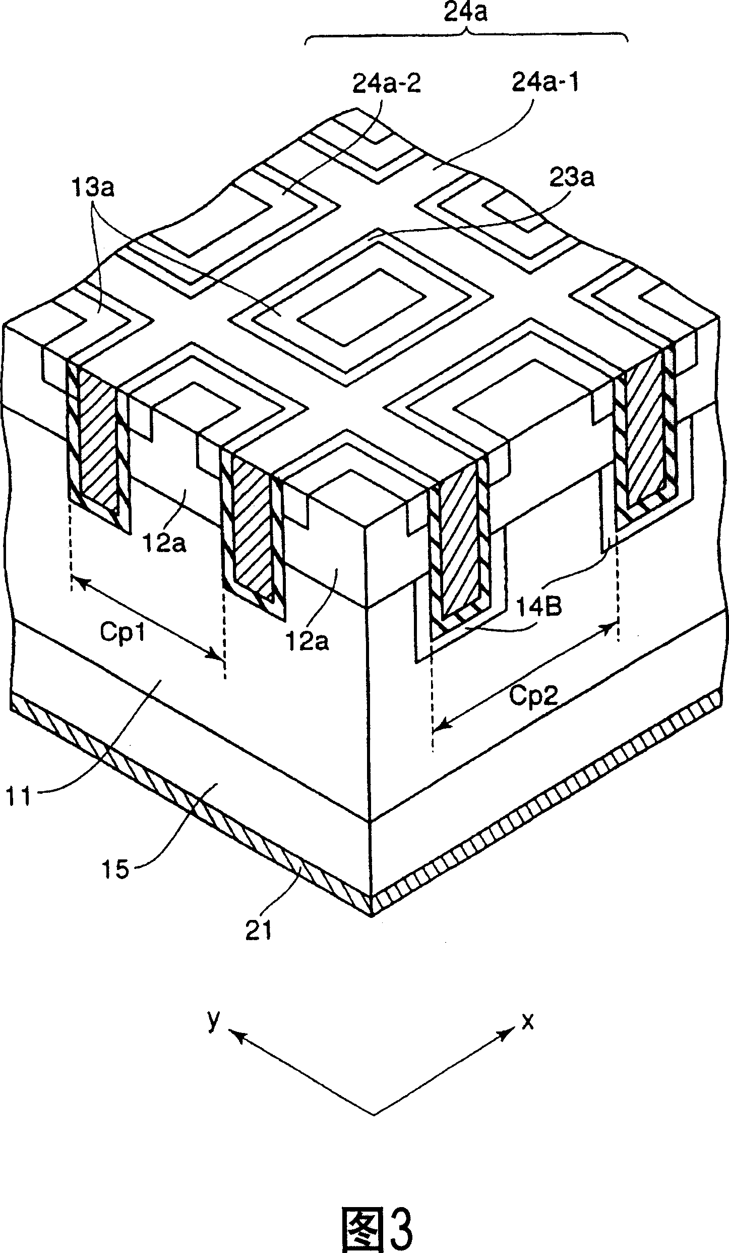
[0042] FIG. 1 is a diagram showing a configuration example of a vertical power MOSFET according to a first embodiment of the present invention. Here, an arbitrary cross section in the x direction (first direction) and an arbitrary cross section in the y direction (second direction) with respect to the vertical power MOSFET are respectively shown. In addition, this embodiment is an example in the case where the gate electrode of the trench structure is formed in a lattice shape.

[0043] In Figure 1, in the n as the first semiconductor layer - On one surface portion of the drift layer 11, a plurality of p base layers 12a are selectively formed as the second semiconductor layer by diffusion. Each p base layer 12a has a rectangular shape and is arranged in a matrix (or zigzag shape). In addition, on the surface portion of each of the above-mentioned p base layers 12a, an n base layer as a third semiconductor layer is selectively formed by diffusion. + source layer 13a. For ex...

no. 2 Embodiment approach

[0063] 10 is a diagram showing a configuration example of a vertical power MOSFET according to a second embodiment of the present invention. Here, an arbitrary cross section in the x direction and an arbitrary cross section in the y direction of the vertical power MOSFET are respectively shown. In addition, this embodiment is an example in the case where the gate electrode of the trench structure is formed in a stripe shape.

[0064] In Fig. 10, in the n as the first semiconductor layer - On one surface portion of the drift layer 11, a plurality of p base layers 12 are selectively formed as the second semiconductor layer by diffusion. The p base layers 12 are arranged in a strip shape with a certain interval (pitch) in the x direction, for example. In addition, on the surface portion of each of the p base layers 12 described above, an n p base layer as a third semiconductor layer is selectively formed by diffusion. + source layer 13. Each n + For example, the source layer...

no. 3 Embodiment approach

[0077] 18 is a diagram showing a configuration example of a vertical power MOSFET according to a third embodiment of the present invention. Here, for example, in n - A case where the n-low resistance layer 11 a is formed on the surface portion of the drift layer 11 .

[0078] The MOSFET of this embodiment passes n - The pn diode (built-in diode) formed by the drift layer and the p base layer can improve the loss and noise when switching from the on state to the off state (recovery time). For example, when MOSFETs are used in power supply circuits such as small inverter circuits (single phase) and bridge circuits, it is known that the loss and noise during recovery of built-in diodes have a large influence on the loss and noise of the power supply circuit.

[0079] That is, in FIG. 18, n as the first semiconductor layer - The drift layer 11 has, on one surface portion thereof, an n low-resistance layer 11a provided by diffusion. In the surface portion of the n low-resistanc...


PUM


Abstract

Insulated gate type semiconductor device. To provide a power MOSFET which is high in speed and is most primarily characterized by having the capability of suppressing switching noise. For example, on the surface of an n-drift layer (11) adjacent to a p-base layer (12a) and an n+-source layer (13a), a gate electrode (24a) in a trench structure is formed in a grid shape. Then, on the boundary of the n-drift layer (11) corresponding to a second electrode (24a-2) crossing a first electrode (24a-1) of the gate electrode (24a), a p-layer (14B) connected to the p-base layer (12a) and having a lower impurity concentration than the p-base layer (12a) has is formed.

Description

technical field [0001] The present invention relates to an insulated gate type semiconductor device for power control, in particular to MOS devices such as power MOSFETs (Metal Oxide Semiconductor Field Effect Transistor: Metal Oxide Semiconductor Field Effect Transistor) and IGBT (Insulated Gate Bipolar Transistor: Insulated Gate Bipolar Transistor) for switching. The gate element or the MIS (Metal Insulator Semiconductor: Metal Insulator Semiconductor) gate element. Background technique [0002] In miniaturization of power supply circuits such as switching power supplies, it is effective to increase the switching frequency. That is, it is effective to reduce passive components such as inductors and capacitors in the power supply circuit. However, if the switching frequency is increased, switching losses of switching elements such as MOSFETs and IGBTs increase. Increased switching losses result in a decrease in power supply efficiency. Therefore, in miniaturization of a ...

Claims


Application Information

Patent Timeline
Patent Type & Authority Patents(China)
IPC IPC(8): H01L29/78H01L29/06H01L29/08H01L29/10H01L29/739
CPCH01L29/7802H01L29/7397H01L29/0847H01L29/1095H01L29/0634H01L29/7813H01L29/0878
Inventor 斋藤涉大村一郎相田聪
Owner KK TOSHIBA
Why Eureka
Try Eureka