Circuit apparatus mfg. method

A technology of circuit device and manufacturing method, which is applied in the fields of circuits, semiconductor/solid-state device manufacturing, electrical components, etc., can solve the problems of difficulty in changing specifications, difficulty in achieving small size, light weight and high performance, and large cost.

Inactive Publication Date: 2004-05-05
SANYO ELECTRIC CO LTD
View PDF2 Cites 2 Cited by
  • Summary
  • Abstract
  • Description
  • Claims
  • Application Information

AI Technical Summary

Problems solved by technology

Among the technologies that provide the system as a package, they are roughly divided into PCB mounting, system LSI, and ISB. It is difficult to achieve small size, light weight, and high performance for PCB mounting, but system LSI can achieve small size, light weight, high performance, and low power consumption. However, it is difficult to change the specifications, and there is a problem that a large amount of cost is required to develop new specifications

Method used


Image

  • Circuit apparatus mfg. method
  • Circuit apparatus mfg. method
  • Circuit apparatus mfg. method

Examples


Embodiment Construction

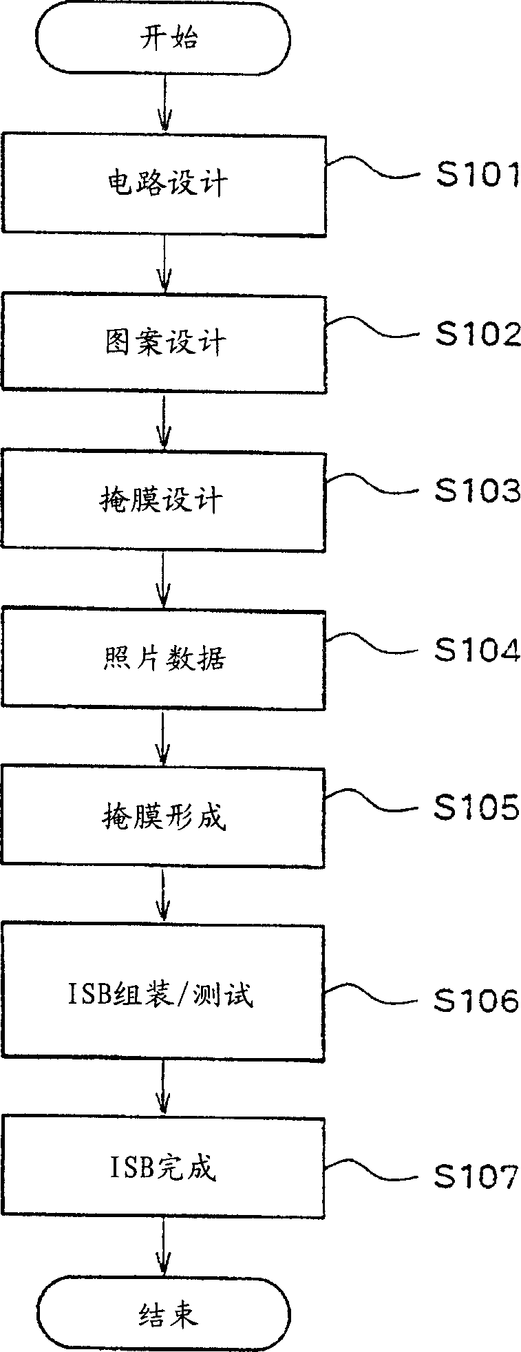
[0044] In the following, the embodiment of the present invention will be described by taking the ISB circuit as an example according to the accompanying drawings. And, if Figure 16 and Figure 17 As shown, the ISB circuit device means a circuit device covered and supported by an insulating resin without a support substrate supporting a plurality of circuit elements (active components and passive components), and most of them include SIP.

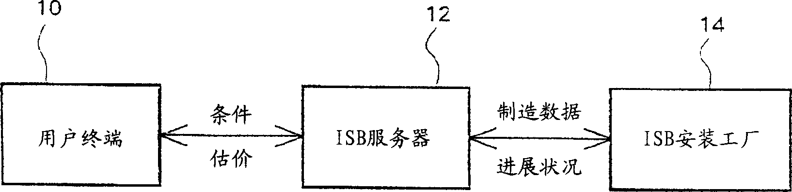
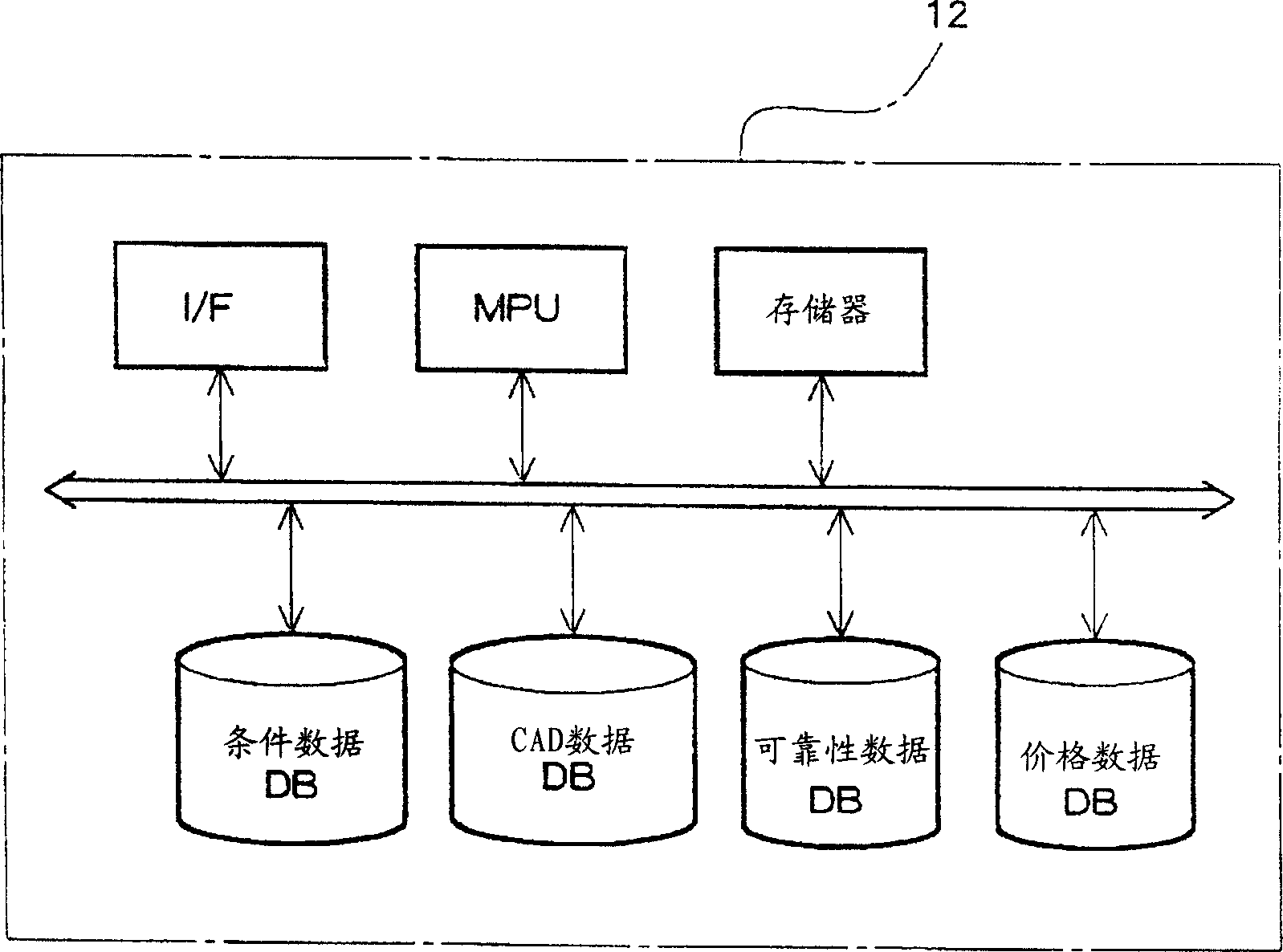
[0045] figure 1 A system configuration diagram showing the ISB circuit device manufacturing system of the present embodiment. The user terminals 10 used by equipment manufacturers of mobile phone manufacturers and home appliance manufacturers are connected to the ISB server 12 through a communication network such as the Internet. Furthermore, the ISB server 12 and the ISB installation factory 14 are also connected by a communication network. The ISB server 12 and the ISB installation factory 14 can also be connected with dedicated lines...


PUM


Abstract

A method of manufacturing a System In Package (SIP) or Integrated System in Board (ISB) circuit device in which a plurality of circuit elements are covered with and integrally supported by an insulating resin. A user terminal is connected with an ISB server and an ISB mounting factory through a communication network. Specifications to be satisfied by an ISB circuit device desired by a user, such as an external size and terminal information of the ISB and circuit diagram CAD data, for example, are input through the user terminal and transmitted to the ISB server. The ISB server in turn transmits information concerning the due date and cost of the ISB circuit device and also a reliability evaluation result to the user terminal. The ISB server also generates mask data for manufacturing the ISB circuit device based on the input specifications, and transmits the mask data to the ISB mounting factory. The ISB mounting factory, receiving the manufacturing data from the ISB server, manufactures the ISB circuit device and provides the ISB circuit device to the user.

Description

technical field [0001] The present invention relates to a method of manufacturing a circuit device, and more particularly to a method of manufacturing a circuit device in which a circuit element without a support substrate is covered and supported by an insulating resin. Background technique [0002] In recent years, instead of packaging one semiconductor element, a technology has been developed to provide multiple circuit elements such as IC, LSI, and chip resistors as a package as a system, called SIP (System in Package) or ISB (Integrated System in Board ). Among the technologies that provide the system as a package, they are roughly divided into PCB mounting, system LSI, and ISB. It is difficult to achieve small size, light weight, and high performance for PCB mounting, but system LSI can achieve small size, light weight, high performance, and low power consumption. However, it is difficult to change the specifications, and there is a problem that a large amount of cost...

Claims


Application Information

Patent Timeline
Patent Type & Authority Applications(China)
IPC IPC(8): H01L25/00G06F17/50H01L21/48H01L23/31H01L25/04H01L25/18
CPCG06F2217/12G06F2217/04G06F17/50H01L2924/3011H01L23/3107H01L2224/45144H01L2224/73265H01L2224/32245G06F2217/40H01L2224/48247H01L21/4832G06F30/00G06F2111/02G06F2113/18G06F2119/18H01L24/73H01L2224/05554H01L2924/181Y02P90/02H01L2924/00012H01L2924/00014H01L2924/00
Inventor 前原荣寿阪本纯次碓氷旭
Owner SANYO ELECTRIC CO LTD
Why Eureka
Try Eureka