Top lighting organic electroluminescent display device

An electroluminescence display and electroluminescence technology, which can be applied to electroluminescence light sources, identification devices, lighting devices, etc., and can solve the problems such as the limitation of the pattern configuration of the light-emitting area and the limitation of the light-emitting area.

Inactive Publication Date: 2005-03-30
SANYO ELECTRIC CO LTD
View PDF1 Cites 2 Cited by
  • Summary
  • Abstract
  • Description
  • Claims
  • Application Information

AI Technical Summary

Problems solved by technology

Due to this, the pattern configuration of the light-emitting area is limited
[0018] In addition, when the pixel electrodes r2, g2, and b2 are covered with an insulating film having an opening, and the light emitting region is determined by the opening, the pattern arrangement of the light emitting region is limited for the same reason as above.

Method used


Image

  • Top lighting organic electroluminescent display device
  • Top lighting organic electroluminescent display device
  • Top lighting organic electroluminescent display device

Examples


Embodiment 1

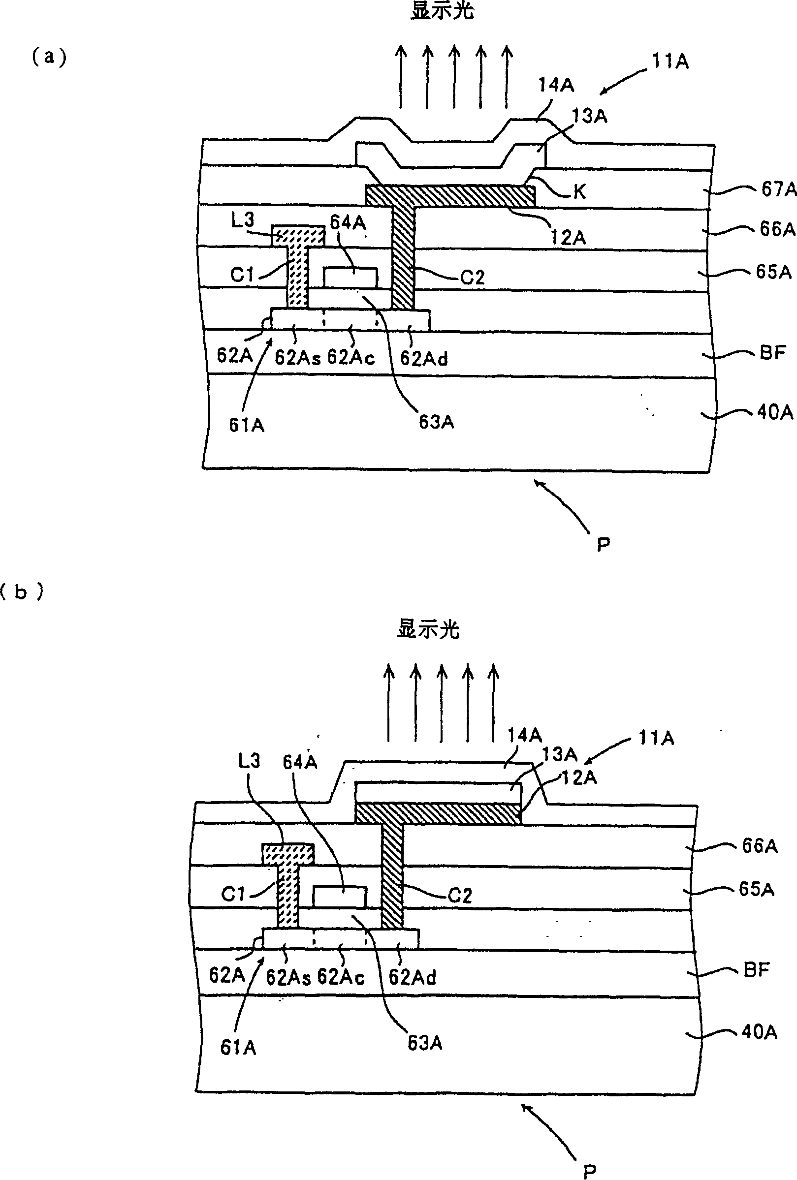
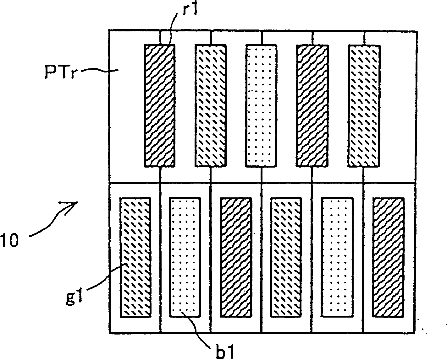
[0082] FIG. 2 is a plan view showing the display portion 10 of the top emission organic electroluminescent display device according to the first embodiment. The TFT formation region PTr of a plurality of display pixels P, that is, the formation region of the driving TFT 61A, the pixel selection TFT 71A, and the storage capacitor Cs is formed in a rectangular shape and arranged in stripes on the display portion 10 . Here, the light-emitting regions r1 , g1 , and b1 of the organic electroluminescent element 11A constituting each display pixel P are formed in a rectangular shape at equal intervals and arranged in a triangular shape across the adjacent TFT formation region PTr.

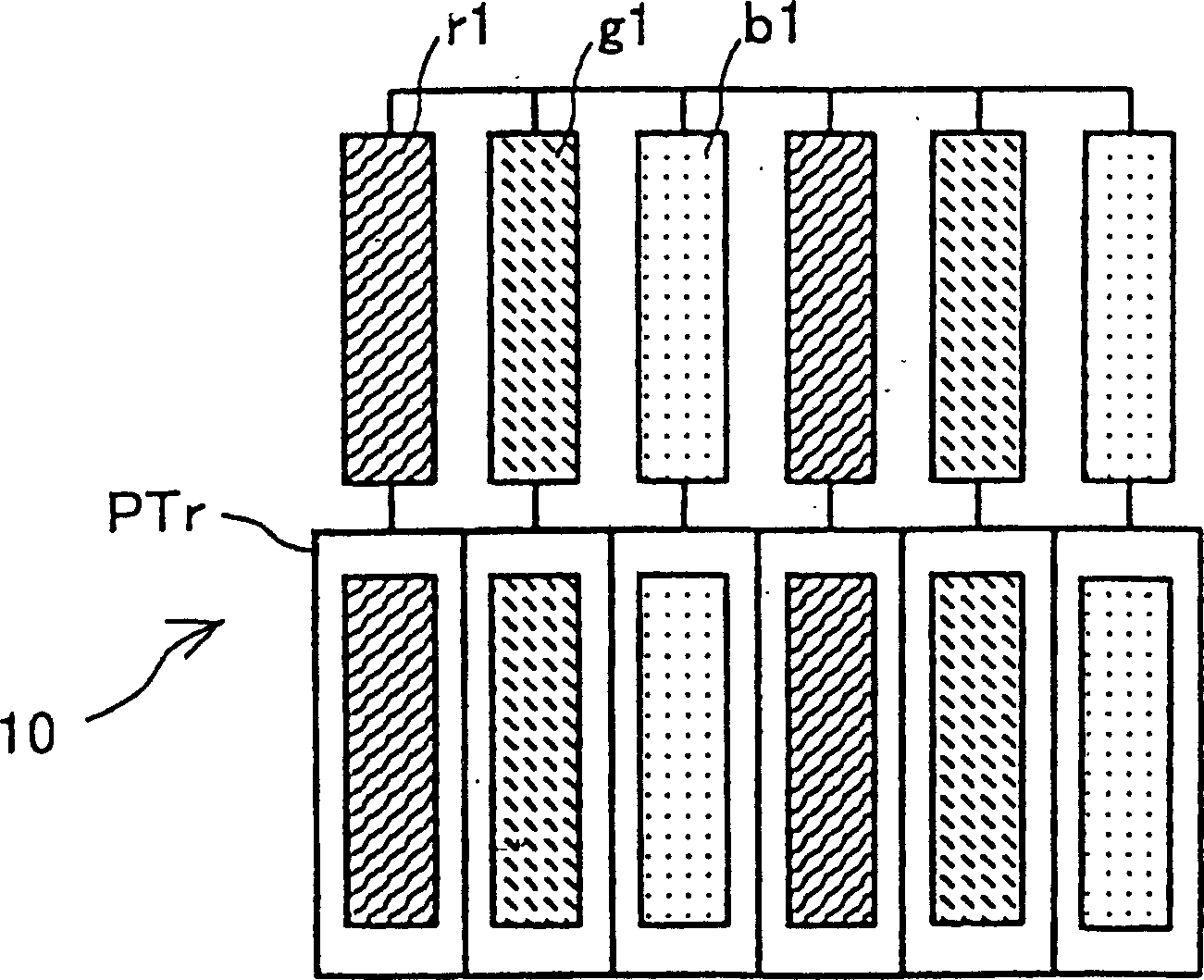
[0083] FIG. 3 is a plan view showing the display portion 10 of the top emission organic electroluminescent display device according to the second embodiment. The plurality of TFT formation regions PTr are formed in a rectangular shape, are arranged offset in the column direction, and are arranged in a tri...


PUM


Abstract

In an organic EL display device, emissive regions are arrayed in various patterns without depending on array patterns of the TFT formation regions and so on. A plurality of TFT formation regions PTr of pixels P is formed in a stripe array on a display portion. Emissive regions R 1 of the organic EL element 11 A emitting red light, emissive regions G 1 of the organic EL element 11 A emitting green light, and emissive regions B 1 of the organic EL element 11 A emitting blue light are arrayed on these TFT formation regions PTr. The emissive regions R 1 , G 1 , and B 1 are disposed in delta array over the adjacent TFT formation regions PTr.

Description

technical field [0001] The present invention relates to an organic electroluminescence (ectro Luminescence; electroluminescence) display device, in particular to an organic electroluminescence display device that improves the degree of freedom in the arrangement position of a light emitting region of an organic electroluminescence component. Background technique [0002] In recent years, organic electroluminescence display devices using electroluminescence (ectro Luminescence) components are attracting attention as display devices replacing CRTs and LCDs. In particular, an organic electroluminescent display device having a thin film transistor (Thin Film Transistor: hereinafter referred to as TFT) as a switch element for driving the organic electroluminescent element has also been developed. [0003] Organic electroluminescent display devices generally have bottom emission (Bottom emission) type and top emission (Top emission) type. Hereinafter, a bottom emission type organ...

Claims


Application Information

Patent Timeline
Patent Type & Authority Applications(China)
IPC IPC(8): H05B33/12G09F9/30G09G3/30H01L27/32H01L29/04H01L51/50H05B33/00H05B33/14
CPCH01L27/3244H01L2251/5315H01L27/3211G09G2300/0452G09G3/3208H10K59/352H10K59/353H10K59/12H10K2102/3026H05B33/00H05B33/12
Inventor 松本昭一郎西川龙司
Owner SANYO ELECTRIC CO LTD
Why Eureka
Try Eureka