Batch treatment apparatus and wafer treatment method

A processing device and wafer processing technology, applied in electrical components, semiconductor/solid-state device manufacturing, circuits, etc., can solve the problems of narrow tolerance margin, large electrical differences, defective products, etc., to reduce the generation of defective products , the effect of reducing the electrical difference

Active Publication Date: 2005-04-20
PROMOS TECH INC
View PDF0 Cites 11 Cited by
  • Summary
  • Abstract
  • Description
  • Claims
  • Application Information

AI Technical Summary

Problems solved by technology

After the wafer 108 has passed through another thermal process, the resistance value measured by the wafer doped with more arsenic will be lower than the resistance value measured by the wafer doped with less arsenic, which will also cause a large electrical difference. The problem
[0008] In a semiconductor process with a wid

Method used


Image

  • Batch treatment apparatus and wafer treatment method
  • Batch treatment apparatus and wafer treatment method
  • Batch treatment apparatus and wafer treatment method

Examples


Embodiment Construction

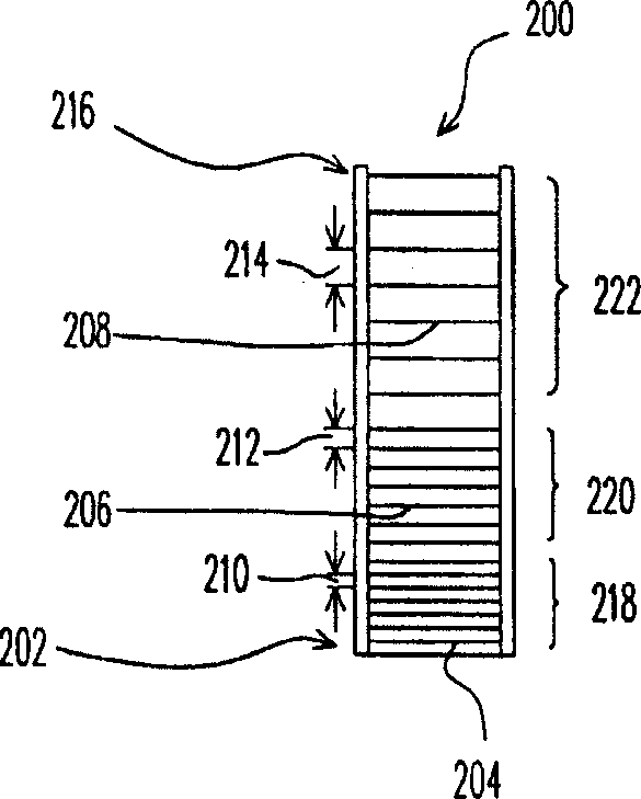
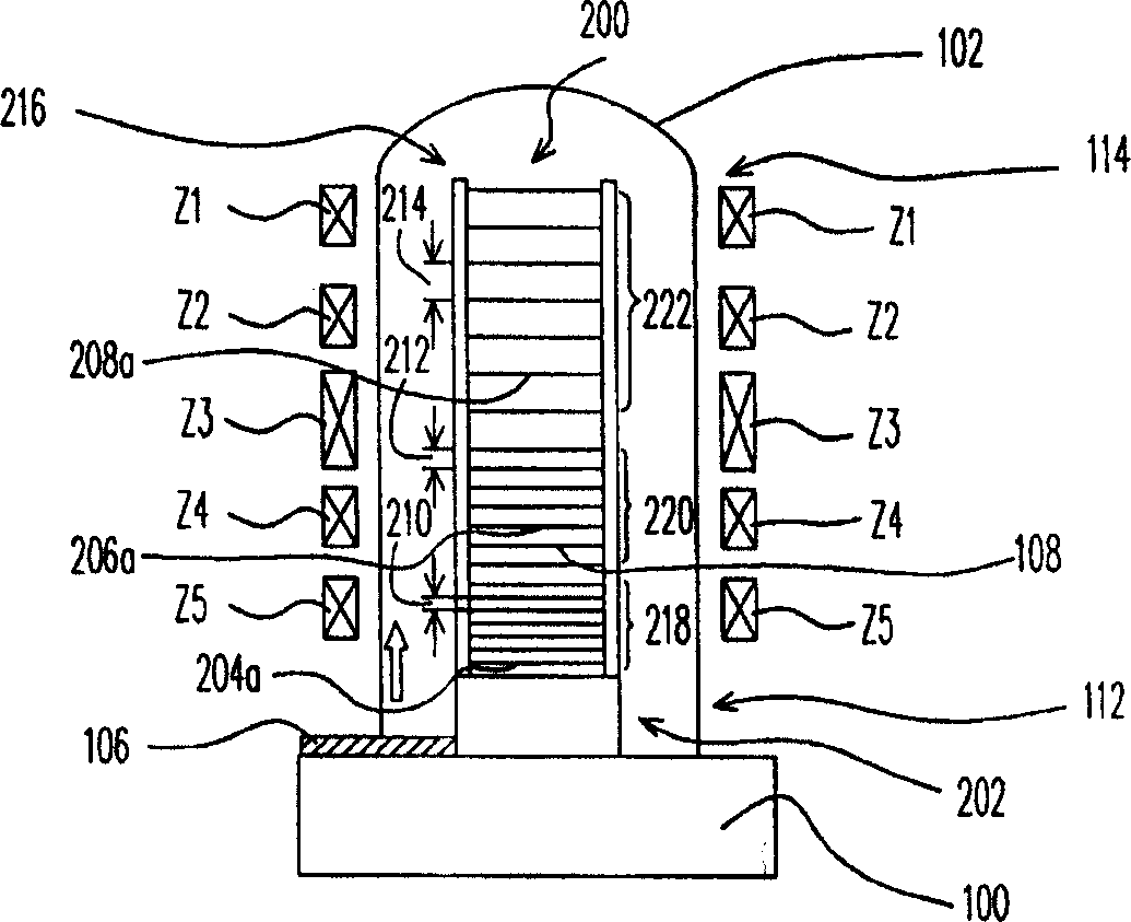
[0033] figure 2 is a schematic cross-sectional view of a wafer boat showing a preferred embodiment of the present invention. Please refer to figure 2 The wafer boat 200 includes a plurality of wafer slots (wafer slots) 204, 206, and 208, wherein the wafer slots 204, 206, and 208 make the wafers (not shown) disposed therein parallel to each other with the surfaces of the wafers, And in the wafer boat 200 , the pitch of the wafer slots gradually increases from the end portion 202 toward the end portion 216 along the direction perpendicular to the wafer surface.

[0034] In this embodiment, the wafer boat 200 is divided into a first portion 218 , a second portion 220 and a third portion 222 from the end portion 202 to the end portion 216 . Wherein the first part 218 has a plurality of wafer slots 204 with the same spacing between the wafer slots 204, and the second part 220 has a plurality of wafer slots 206 with the same spacing between the wafer slots 206, The third part 2...


PUM


Abstract

This invention provides a batch process device and wafer process method, in which, the batch process device includes a crystal boat, multiple slots for wafers are set between the first end and the second end enabling surfaces of wafers matched in them parallel to each other, distance between slots is increased from the first end towards the second end steadily, a gas inlet providing gas from the first end towards the second end to let the gas react with the wafers. The crystal boat can be matched in vertical heat oven pipe, the first end is on the bottom and the second part is set at the top. Wafers processed with this vertical heat oven tube can reduce electric difference among the same batch of processed wafers.

Description

technical field [0001] The present invention relates to a semiconductor device and a manufacturing method, and in particular to a wafer boat, a batch type processing device and a wafer processing method using the wafer boat. Background technique [0002] The furnace tube reactor is a batch processing device, so a large number of wafers can be processed at one time, and the furnace tube reactor can be applied to chemical vapor deposition (Chemical Vapor Deposition, CVD) process and doping (Doping) process . In the application of chemical vapor deposition process, it is mainly used for the deposition of materials such as polysilicon, silicon oxide and silicon nitride. As for the application of doping process, it can be applied to the gate polysilicon layer of metal oxide semiconductor transistors, for example. Dopant presets, etc. Furnace tube reactors can be mainly divided into two types: horizontal type and vertical type. Due to the small overall volume required by the ver...

Claims


Application Information

Patent Timeline
IPC IPC(8): H01L21/205H01L21/22
Inventor 林焕顺
Owner PROMOS TECH INC
Why Eureka
Try Eureka