
PCB fastener

A technology of circuit boards and fixing frames, which is applied in the direction of identification devices, electrical components, and structural parts of electrical equipment, etc., can solve problems such as easy to generate errors and cannot provide horizontal pinching and tightening effects, and achieve tight joints and good uniformity display quality effects

Inactive Publication Date: 2005-05-11
HARVATEK CORPORATION
View PDF0 Cites 0 Cited by
  • Summary
  • Abstract
  • Description
  • Claims
  • Application Information

AI Technical Summary

Problems solved by technology

[0004] However, attention should be paid to the accuracy of the distance between the two screw holes of the fixing piece 14a, and the accuracy with which the screw seats 111a, 112a are arranged on the circuit boards 101a, 102a; Afterwards, errors are prone to occur, and the tightening device is a fixed-distance positioning joint, and the locking direction is vertical up and down, which cannot provide the tightening effect of horizontal pinching; if Figure 1B As shown, the circuit boards 101a, 102a have a slight angle θ due to the combination tolerance; or refer to Figure 1C As shown, in case of improper horizontal shear force F, it is easy to cause the relative displacement x of the circuit boards 101a and 102a

Method used


Image

  • PCB fastener
  • PCB fastener
  • PCB fastener

Examples


Embodiment Construction

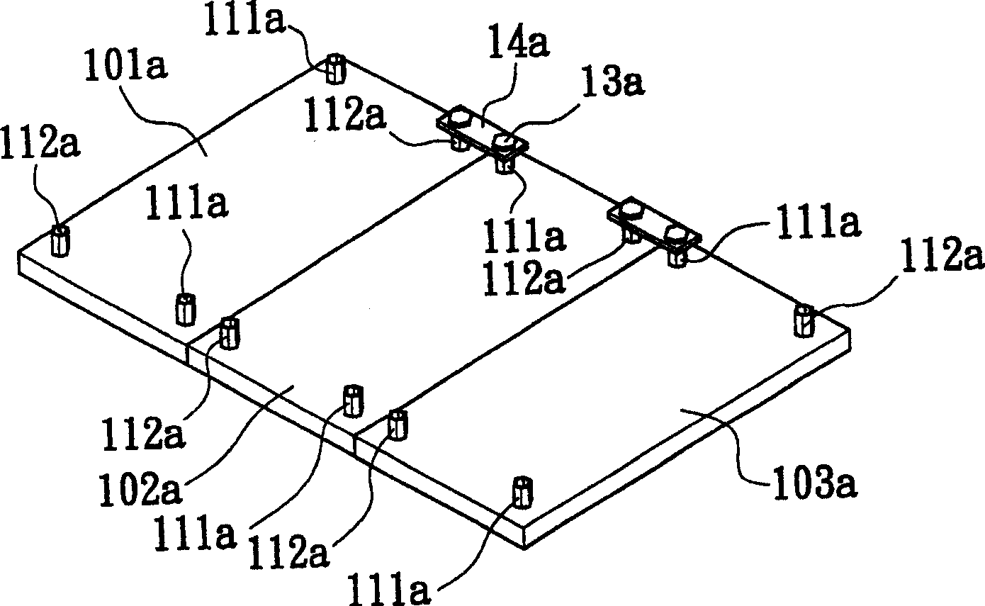
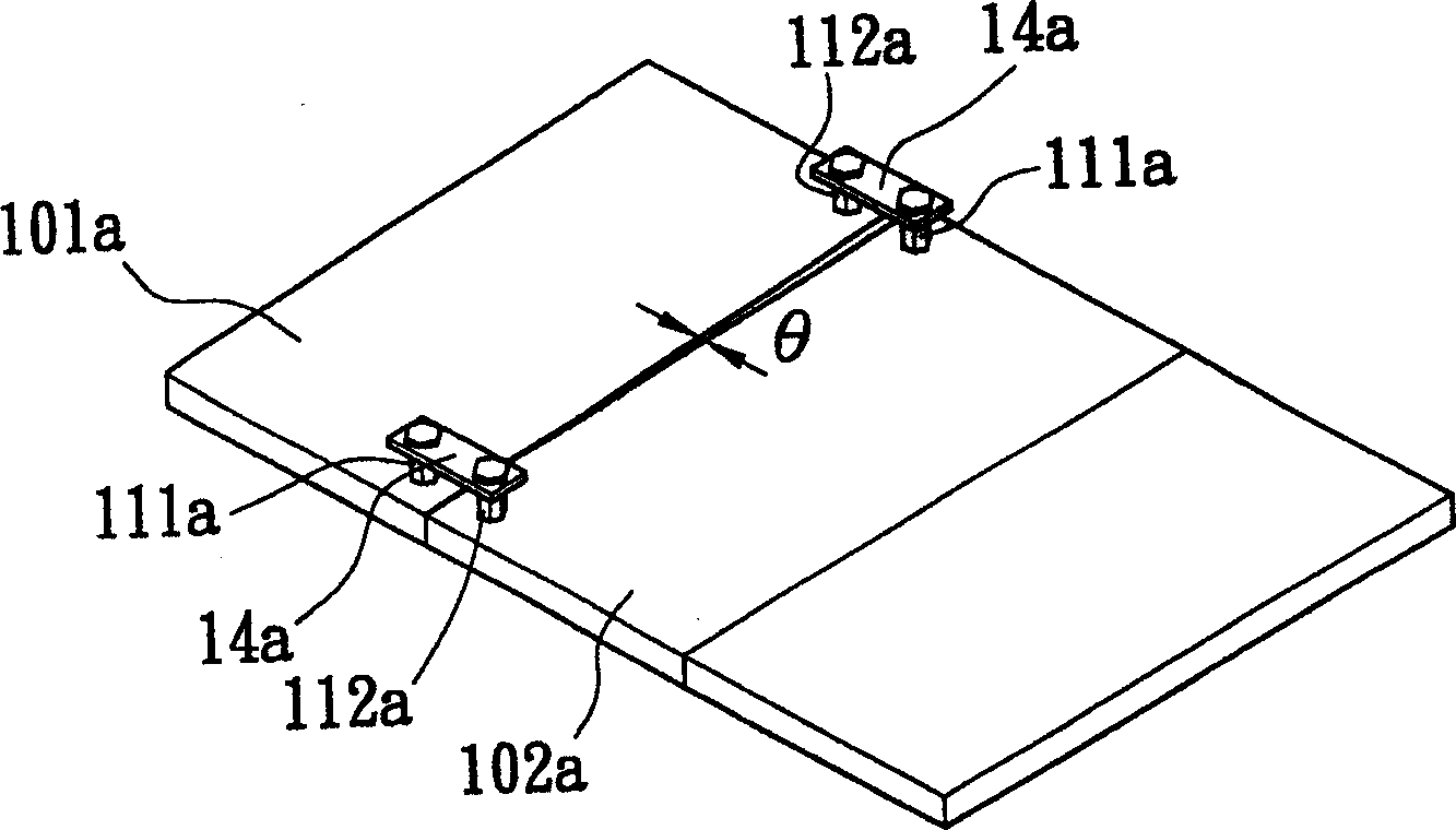
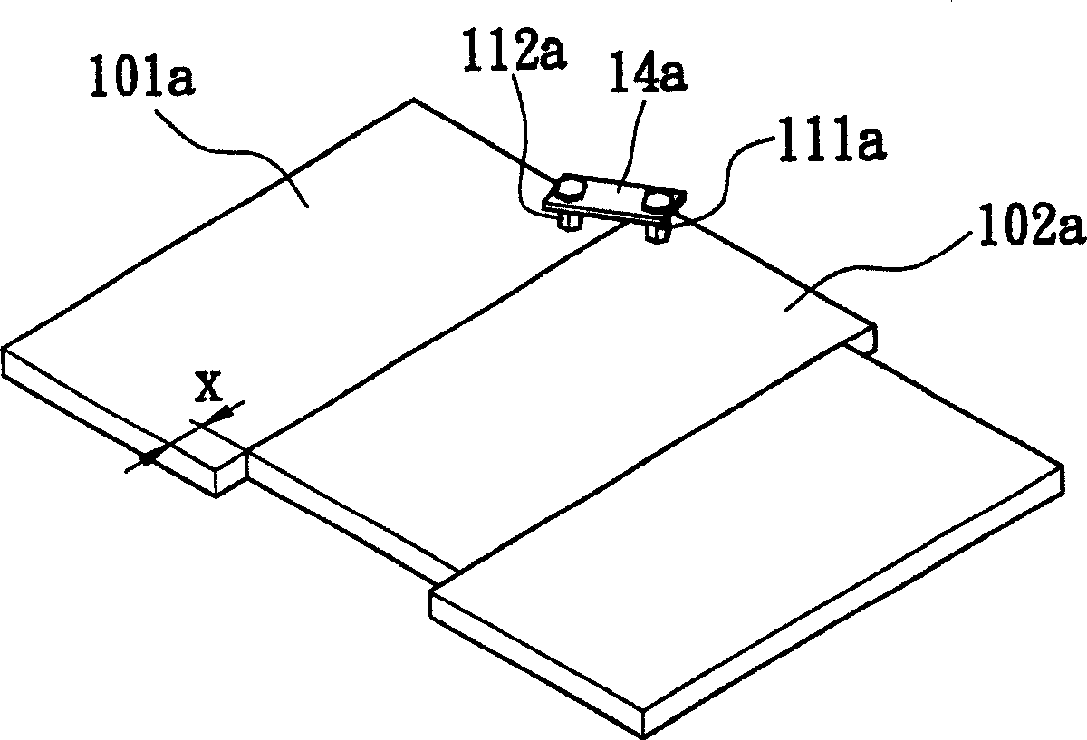
[0042] The present invention utilizes the L-shaped fixing frame connected to the circuit board by the U-shaped tenon clip to provide a tightening effect that the circuit board is clamped horizontally to the center line, so as to achieve good and uniform display quality of the light-emitting diode display.

[0043] Please refer to figure 2 As shown, it is the first embodiment of the circuit board clamping device of the present invention. In order to achieve a uniformly displayed light-emitting diode display screen, it includes a plurality of circuit boards 10 adjacent to each other, which are respectively fixed on the circuit boards 10. Multiple pairs of L-shaped fixing frames 21, at least one U-shaped tenon 22 holding the pair of L-shaped fixing frames 21, are used to forcefully combine two adjacent circuit boards 10; wherein, the circuit board 10 has a set The information display surface (not shown) of the light-emitting diode matrix, and the holding surface 101 relative to ...


PUM


Abstract

A clamping device of circuit board for LED display screen consists of multiple circuit boards to be connected in two adjacent pieces to two adjacent two pieces, L shaped fixture on circuit board U shaped trip checked with L shaped fixture. It features that U shaped trip is clamped with L shaped fixture connected on the circuit board to provide clamping force towards middle line along circuit board level direction.

Description

technical field [0001] The invention relates to a circuit board pressing device, in particular to a circuit board pressing device applied to a light-emitting diode display screen. Background technique [0002] A large light emitting diode display (Light Emitting Diode Display, LED Display) is composed of multiple light emitting diode matrix units. The aforementioned light emitting diodes are respectively placed on multiple circuit boards and arranged in a matrix to display information; In order to meet the size requirements of the large screen, multiple circuit boards must be connected in pairs, and the tight fit between the circuit boards must be accurately controlled to prevent the displayed information from affecting the display uniformity and quality due to the spacing between the circuit boards. [0003] Please refer to Figure 1A As shown, it is a known technology pressing circuit board device, which is applied to multi-chip circuit boards 101a, 102a and 103a with both...

Claims


Application Information

Patent Timeline
IPC IPC(8): G09F9/30H05K7/00
Inventor 汪秉龙庄峰辉林惠忠
Owner HARVATEK CORPORATION
Features
  • Generate Ideas
  • Intellectual Property
  • Life Sciences
  • Materials
  • Tech Scout
  • Unparalleled Data Quality
  • Higher Quality Content
  • 60% Fewer Hallucinations
Learn More