Display with integrated electrodes

a technology of light-emitting diodes and integrated electrodes, which is applied in the direction of optics, instruments, electric digital data processing, etc., can solve the problems of more limited touch modes, high-resolution photolithographic processes over large substrates, and process steps that require expensive high-resolution photolithographic processes, etc., and achieve the effect of reducing the thickness of the touch screen

Active Publication Date: 2017-04-13
X DISPLAY CO TECH LTD
View PDF13 Cites 80 Cited by
  • Summary
  • Abstract
  • Description
  • Claims
  • Application Information

AI Technical Summary

Benefits of technology

[0008]The present invention provides an inorganic light-emitting diode (iLED) display with integrated electrodes. The iLEDs form pixels that are located over a display area of a display surface to form the display and are interconnected in rows by electrical conductors that provide power, ground, and control signals to operate the pixels in the display. Row touch electrodes are disposed in rows over the display surface in the display area between the rows of light emitters. The row touch electrodes provide at least some of the elements of a touch screen, for example the row touch electrodes of a projected mutual-capacitance touch screen. The row touch electrodes and the electrical conductors can be located in a common plane, reducing the thickness of a touch screen, since both the row touch electrodes and the iLEDs are formed in rows in the display area.
[0009]In another arrangement of the present invention, an inorganic light-emitting diode display with integrated electrodes includes a display surface having a display area and a plurality of spatially separated inorganic light-emitting diodes (iLEDs) disposed on the display surface in the display area. A plurality of row touch electrodes is disposed in rows over the display surface in the display area between the inorganic light-emitting diodes in a direction parallel to the display surface and a plurality of column touch electrodes are disposed in columns over the display surface in the display area between the inorganic light-emitting diodes in a direction parallel to the display surface. This construction eliminates the need for transparent electrodes and thereby reduces costs and increases electrode conductivity, improving the operating frequency of the electrodes and size of the touch screen.
[0010]In another embodiment of the present invention, a display with an integrated touch screen includes an array of light emitters in a display area of a display surface with one or more sensing elements of a touch screen. The sensing elements are disposed either in a common plane with the light emitters or disposed on a side of the light emitters opposite the display surface. Because the sensing elements are not located between a display viewer and the light emitters, the sensing elements, such as electrodes, do not need to be transparent. Thus, the electrodes can include opaque, highly conductive materials, for example thick metal traces rather than relatively low-conductance metal oxides such as indium tin oxide or spaced-apart micro-wires. The highly conductive electrodes have a lower capacitance and can be operated at a higher frequency, enabling faster and larger touch screens with an improved signal-to-noise ratio.
[0012]In any of these embodiments, the electrodes are located between the light emitters in a direction parallel to the display surface and therefore do not obscure light emitted from the light emitters toward a display viewer nor does light emitted from the light emitters have to pass through the electrodes. Thus, there is no need for the electrodes to be transparent and they can therefore be made of more-conductive materials than are found in devices, such as touch screens, used with displays and found in the prior art. This structure and the materials provide the advantages of a wider selection of materials and manufacturing processes and increased conductivity. The increased conductivity enables larger devices operated at a higher frequency and with more sensitive or powerful operation since the reduction in electrical resistance enables greater currents, stronger electro-magnetic fields, and an improved signal-to-noise ratio for current sensing. Moreover, structures of the present invention can be thinner and lighter than prior-art designs.

Problems solved by technology

In contrast, multi-touch touchscreens, for example self-capacitive or mutual-capacitive touch sensors, can detect multiple touch points on a screen at a time but are more limited in their touch modalities, for example limited to touches with a conductive stylus, such as a human finger.
Furthermore, the process steps can require expensive high-resolution photolithographic processes over large substrates.

Method used


Image

  • Display with integrated electrodes
  • Display with integrated electrodes
  • Display with integrated electrodes

Examples


Embodiment Construction

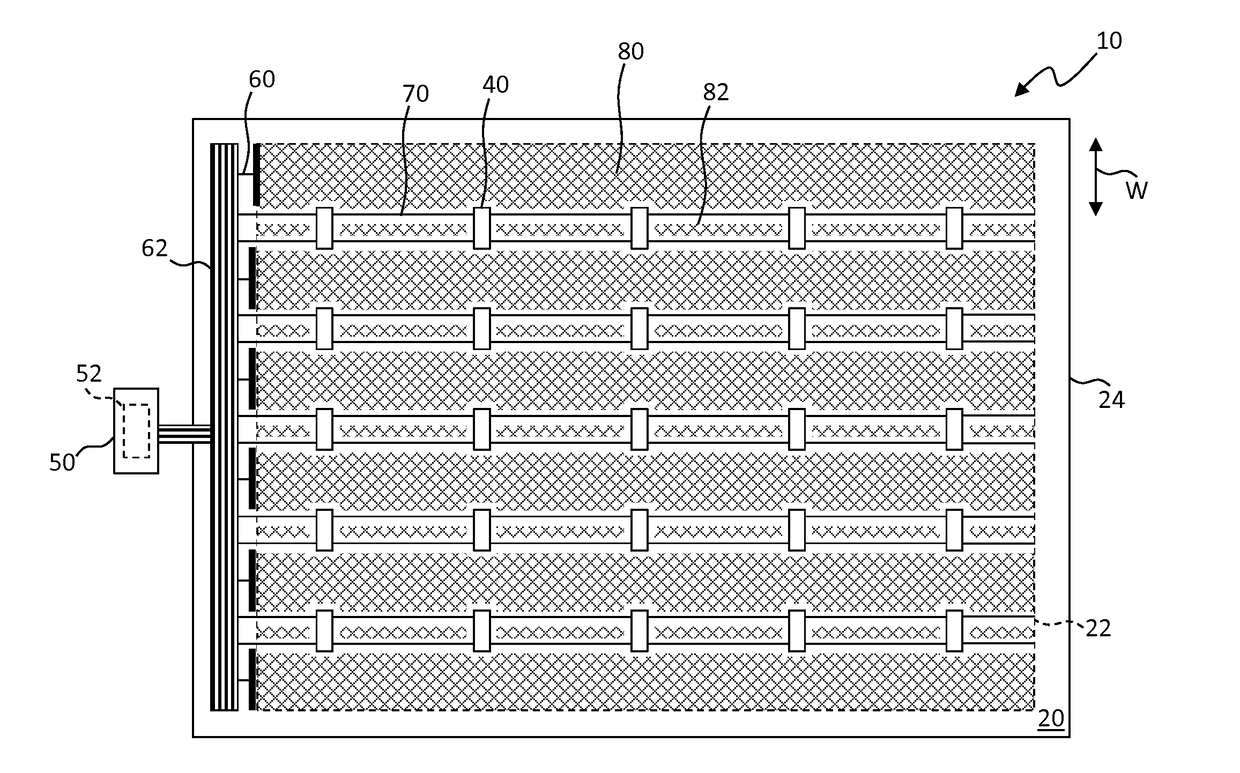
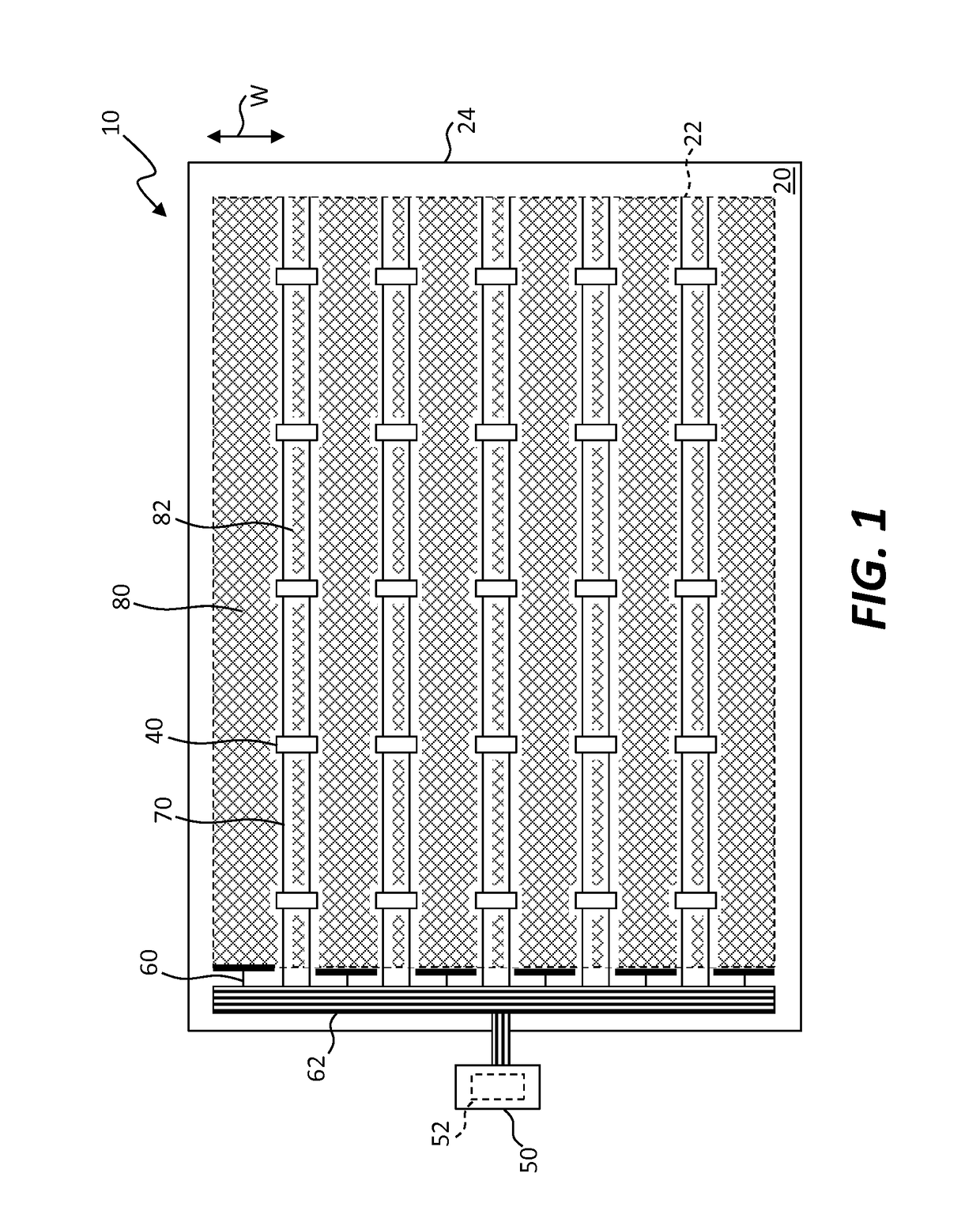
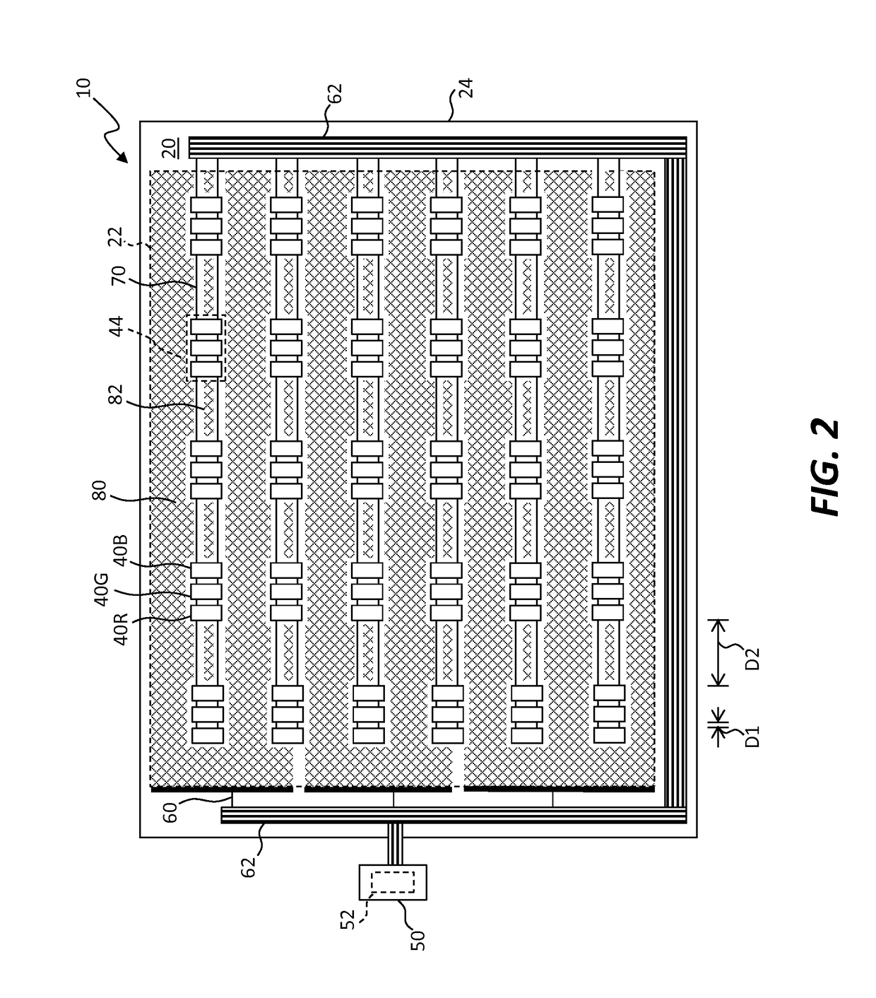
[0121]Referring to FIG. 1, in an embodiment of the present invention, a light-emitting diode display 10 with integrated touch electrodes 80 includes a display surface 20 having a display area 22. The display surface 20 can be a surface of a display substrate 24 and the display area 22 is the portion of the display surface 20 that is used to electronically display information for viewing by a display viewer (e.g. display viewer 99, FIG. 4). A plurality of spatially separated light-emitting diodes (LEDs) 40 is disposed in rows on or in the display surface 20 in the display area 22, for example in a direction parallel to the display surface 20. The light-emitting diodes 40 can be organic light-emitting diodes, inorganic light-emitting diodes, or a combination of organic and inorganic light-emitting diodes. In an embodiment, all of the light-emitting diodes 40 are inorganic light-emitting diodes. The light-emitting diodes 40 in each row of light-emitting diodes 40 are electrically conne...


PUM


Abstract

An inorganic light-emitting diode display with integrated electrodes includes a display surface having a display area and a plurality of spatially separated light-emitting diodes (such as inorganic light-emitting diodes) disposed in rows on the display surface in the display area. The inorganic light-emitting diodes in each row of inorganic light-emitting diodes are electrically connected by one or more electrical conductors. One or more row touch electrodes are disposed in rows over the display surface in the display area between the rows of inorganic light-emitting diodes and are disposed on the display surface and have a width that is larger than a length and width of the light-emitting diodes. A display with an integrated touch screen includes one or more sensing elements disposed in a common plane with the light emitters or on a side of the light emitters opposite the display surface.

Description

CROSS REFERENCE TO RELATED APPLICATIONS[0001]Reference is made to commonly assigned U.S. patent application Ser. No. 14 / 754,573 filed Jun. 29, 2015, entitled Small-Aperture-Ratio Display with Electrical Component, U.S. patent application Ser. No. 14 / 823,917, filed Aug. 11, 2015, entitled Printable Component Structure with Electrical Contact, U.S. patent application Ser. No. 14 / 743,981, filed Jun. 18, 2015, entitled Micro Assembled Micro LED Displays and Lighting Elements, and U.S. patent application Ser. No. 14 / 822,868, filed Aug. 10, 2015, entitled Compound Micro-Assembly Strategies and Devices, the contents of each of which is incorporated by reference herein in its entirety.FIELD OF THE INVENTION[0002]The present invention relates to an inorganic light-emitting diode display having integrated electrodes useful for touch sensing.BACKGROUND OF THE INVENTION[0003]Flat-panel displays are widely used in conjunction with computing devices, in portable devices, and for entertainment dev...

Claims


Application Information

Patent Timeline
Patent Type & Authority Applications(United States)
IPC IPC(8): G06F3/044G06F3/041
CPCG06F3/0412G06F3/044G02F1/13318G02F1/13338G02F1/133553G02F1/133603G02F2201/50G02F2203/02G06F2203/04111G06F2203/04112G09G2354/00G09G2300/0426G06F3/04164G06F3/0446G06F3/0443G06F3/0445G02F1/133601G02F1/133616H01L25/0753H01L33/62H01L25/167H01L33/60G09G3/32
Inventor COK, RONALD S.
Owner X DISPLAY CO TECH LTD
Why Eureka
Try Eureka