
Printed circuit board blind hole quality analysing method

A printed circuit board, quality analysis technology, applied in the direction of mechanically removing conductive materials, measuring devices, instruments, etc., can solve problems such as unsatisfactory and incomplete presentation of laser blind holes

Active Publication Date: 2005-07-20
MACHVISION INC
View PDF1 Cites 19 Cited by
  • Summary
  • Abstract
  • Description
  • Claims
  • Application Information

AI Technical Summary

Problems solved by technology

[0008] Since the known technology cannot fully present the characteristics of the above-mentioned various states of the laser blind hole on the printed circuit board, it cannot meet the needs of the current industry

Method used


Image

  • Printed circuit board blind hole quality analysing method
  • Printed circuit board blind hole quality analysing method
  • Printed circuit board blind hole quality analysing method

Examples


Embodiment Construction

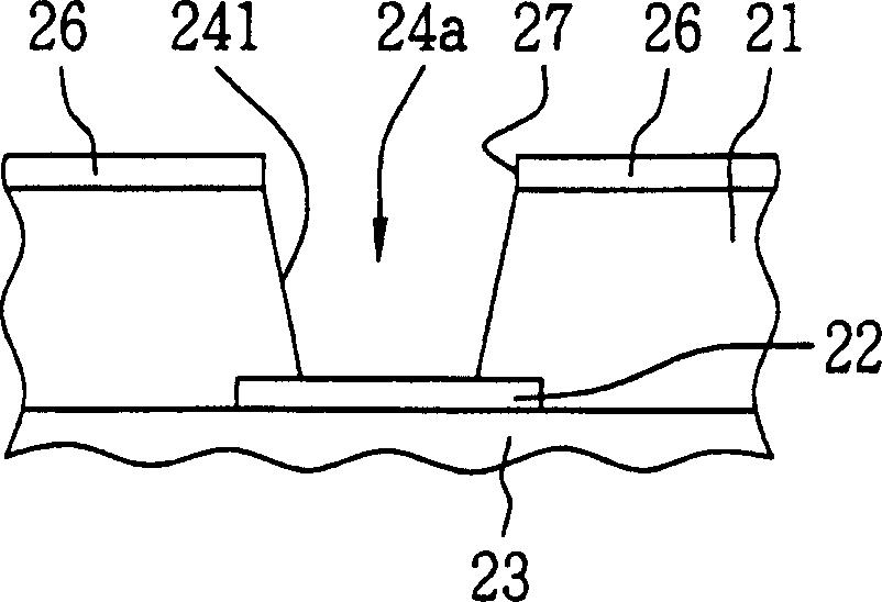
[0024] image 3 is a flowchart of the present invention. As shown in step 31, the original design data of the printed circuit board and the measurement data of the finished product are input, for example: the ideal hole position coordinates (X, Y) of the design, the hole position coordinates (Xo', Yo') of the measured copper window, the measured The pad hole position coordinates (Xp i ', Yp i ′) (i is the number of pads), the designed copper window radius r o , Measured copper window radius r o ′, the designed pad integration radius r p , The measured pad average radius r p ′, the designed hole roundness P, the measured hole roundness P′2 of the copper window, the measured pad hole roundness P′3, the area and coordinates of the residual glue and other data. Then proceed to step 32, using the above-mentioned input data to calculate statistical data, for example: the deviation of the hole position (ΔX, ΔY), wherein ΔX=X-Xo' and ΔY=Y-Yo'; copper window and pad Radius deviat...


PUM


Abstract

The invention reveals a PCB (printed circuit board) blind hole quality analyzing method, firstly inputting design data of manufacturing laser blind holes on the PCB and actual measured data, and using the design data and measured data to calculate various statistical quantities. The expressing modes of these statistical quantities include target diagram, hole position deviation distribution diagram, vector diagram, pad area ratio distribution diagram and remaining glue area ratio distribution diagram, and it can display copper window message, pad message and relative message of pad by these diagrams. Finally, by these messages, it can clearly show manufacturing quality of laser blind holes on the PCB.

Description

technical field [0001] The invention relates to a method for analyzing the quality of blind holes of printed circuit boards, in particular to a method for clearly presenting the distribution state of processing accuracy of laser blind holes on printed circuit boards. Background technique [0002] Printed circuit boards are the main components of electronic products such as computers and communications. In order to adapt to the characteristics of light, thin, short and small products in the consumer market, driven by the demand for high density and high reliability, most advanced printed circuit boards are currently Blind hole (via) and buried hole (buried hole) techniques have been used. This kind of printed circuit board with blind holes and buried holes connects the internal wiring boards with the surface wiring through blind holes, and does not need to penetrate the entire board to waste the layout space of other layer wiring boards. It is estimated that it can be compare...

Claims


Application Information

Patent Timeline
IPC IPC(8): G01B21/00H05K3/04
Inventor 汪光夏萧武域苏家禾洪英凯
Owner MACHVISION INC
Features
  • Generate Ideas
  • Intellectual Property
  • Life Sciences
  • Materials
  • Tech Scout
  • Unparalleled Data Quality
  • Higher Quality Content
  • 60% Fewer Hallucinations
Learn More