Method of repairing disconnection, method of manufacturing active matrix substrate by using thereof, and display device

An active matrix and substrate technology, applied in the field of display devices and manufacturing active matrix substrates, can solve the problems of display defects, data signal wiring affecting pixel electrode voltage, etc., and achieve the effect of reducing display defects and improving output

Inactive Publication Date: 2006-11-15
NEC LCD TECH CORP
View PDF1 Cites 12 Cited by
  • Summary
  • Abstract
  • Description
  • Claims
  • Application Information

AI Technical Summary

Problems solved by technology

Since these conductive particle dense and connected regions formed by laser CVD are conductive, additional parasitic capacitance is caused between the pixel electrode and the part where the broken wiring has been repaired
Therefore, this brings about the problem of causing display defects because the repaired data signal wiring affects the pixel electrode voltage

Method used


Image

  • Method of repairing disconnection, method of manufacturing active matrix substrate by using thereof, and display device
  • Method of repairing disconnection, method of manufacturing active matrix substrate by using thereof, and display device
  • Method of repairing disconnection, method of manufacturing active matrix substrate by using thereof, and display device

Examples


Embodiment Construction

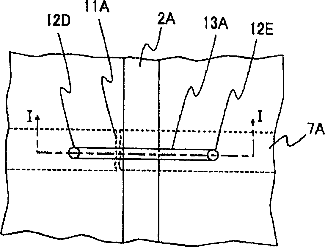
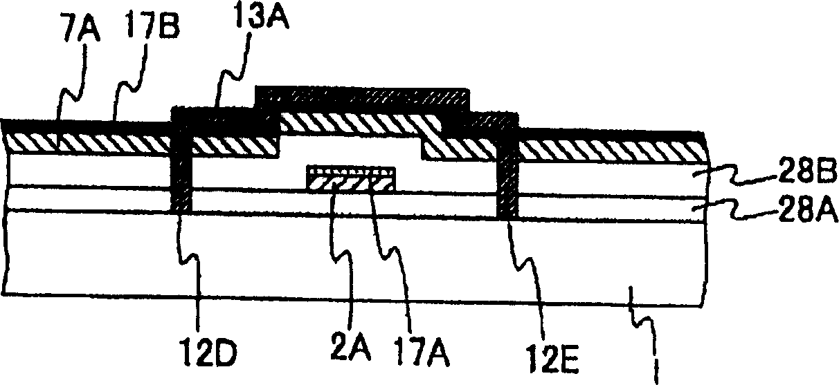
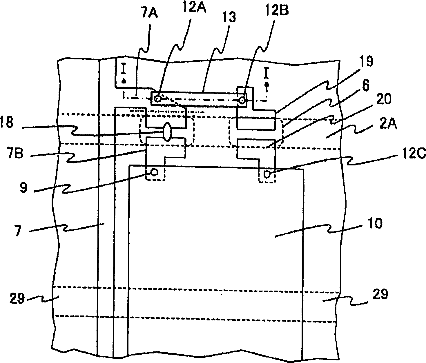
[0038] Referring to the accompanying drawings, a detailed description will be provided of preferred embodiments of the present invention. In order to make the present invention easy to understand, first, reference will be made to Figures 15A to 15D and 16A to 16C, provide descriptions of the method of manufacturing the active matrix liquid crystal display device except for the step of repairing the disconnection defect portion. Figures 15A to 15D and 16A to 16C show an example of a method of manufacturing an active matrix liquid crystal display device including an active matrix substrate (TFT substrate) with a process called back channel etch. ) TFT of inverted staggered (inverted staggered) TFT.

[0039] First, a metal film having a thickness of approximately 200 nm to 300 nm is formed on a transparent insulating substrate 1 such as a glass substrate, such as Figure 15A shown. This metal film is patterned by photolithography and etching techniques. Thus, scanning signa...


PUM

PropertyMeasurementUnit
thicknessaaaaaaaaaa
thicknessaaaaaaaaaa
thicknessaaaaaaaaaa

Abstract

A part where a wiring is disconnected is repaired by the laser CVD method while active matrix substrates for liquid crystal display devices and organic electroluminescence display devices are being manufactured. By the laser CVD method, a conductive film is selectively formed in the part where the wiring is disconnected. Thereafter, laser light is irradiated on at least a surrounding area of the conductive film, and thus conductive fine particles remaining in the surrounding area of the conductive film are removed therefrom. As a result, a leak current and parasitic capacity can be inhibited from occurring between the part where the disconnection has been repaired and another wiring.

Description

technical field [0001] The present invention relates to a method for repairing disconnection of wiring formed on a substrate. In particular, the present invention relates to a method of manufacturing an active matrix substrate using the method of repairing a disconnection, and to a display device including the same method. Background technique [0002] Liquid crystal display devices using thin film transistors (hereinafter referred to as "TFTs") as switching elements have been widely used. Amorphous silicon (hereinafter referred to as "a-Si") is mainly used for semiconductor films of TFTs. In addition, a liquid crystal display device using polysilicon for a semiconductor film of TFT has been commercialized. Further, organic electroluminescence display devices in which pixel circuits are composed of polysilicon TFTs have been developed. [0003] Active matrix display devices such as liquid crystal display (LCD) devices and organic electroluminescent (EL) display devices al...

Claims


Application Information

Patent Timeline
Patent Type & Authority Applications(China)
IPC IPC(8): G02F1/13G02F1/136H05B33/00
CPCG02F1/136259G02F1/136286H01L27/124
Inventor 大石三真
Owner NEC LCD TECH CORP
Why Eureka
Try Eureka