
Transversing cathode emitting structural panel display device and its production technique
A flat-panel display and cathode emission technology, which is applied in cross-cutting fields, can solve problems such as large emission current, high density of carbon nanotubes, and use restrictions, so as to avoid short-circuit phenomenon and improve the production success rate.
- Summary
- Abstract
- Description
- Claims
- Application Information
AI Technical Summary
Problems solved by technology
Method used
Image

Examples
Embodiment Construction
[0038]The present invention will be further described below in conjunction with the accompanying drawings and embodiments, but the present invention is not limited to these embodiments.
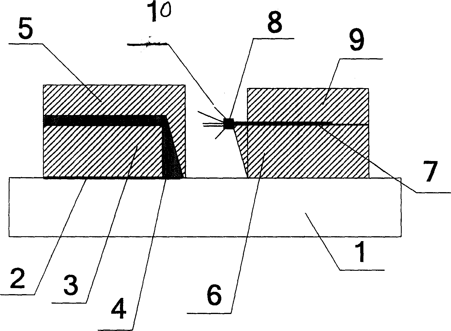
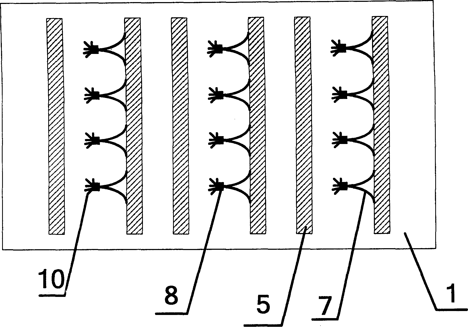
[0039] Described a kind of flat-panel display with horizontal cathode emission structure, comprises the airtight vacuum cavity that is made of cathode glass panel 1, anode glass panel 11 and surrounding glass enclosure frame 16; On the anode glass panel, anode conductive layer 12 and A phosphor layer 14 prepared on the anode conductive layer; a grid 4, a carbon nanotube 10 cathode and a lateral cathode emission structure are arranged on the cathode glass panel; a support wall structure 15 and a gas getter between the anode glass panel and the cathode glass panel Agent attachment 17.
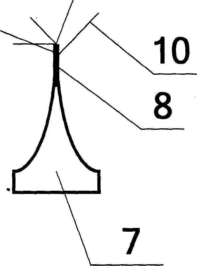
[0040] The horizontal cathode emitter structure includes a cathode glass panel 1, a grid lead layer 2, a grid booster layer 3, a grid layer 4, a grid cover layer 5, a cathode booster layer 6, a cathode conductiv...
PUM
 Abstract
Description
Claims
Application Information