Semiconductor device and method of manufacturing the same

a technology of magnetic resistor and semiconductor, which is applied in the direction of magnetic field-controlled resistor, semiconductor device, electrical apparatus, etc., can solve the problems of short circuit failure of magnetic resistor elements, and achieve the effect of reducing short circuit failures

Inactive Publication Date: 2011-03-03
RENESAS ELECTRONICS CORP
View PDF4 Cites 52 Cited by
  • Summary
  • Abstract
  • Description
  • Claims
  • Application Information

AI Technical Summary

Benefits of technology

[0013]In the semiconductor device according to the embodiment of the present invention, the surface of the first portion of the first insulating film located in the first region where the magnetic resistor elements are formed is at the position lower than that of the surface of the second portion of the first insulating film located in the second region. This ensures a thickness to the portion of the second insulating film located in the first region and in the vicinity of the boundary between the first region and the second region, and inhibits the magnetic resistor element located at the end of the first region in the vicinity of the boundary from being damaged by etching when the first wire grooves are formed in the second insulating film or the like. As a result, it is possible to reduce short circuit failures in the magnetic resistor elements and the like.
[0014]In the method of manufacturing the semiconductor device according to the embodiment of the present invention, the surface of the first portion of the first insulating film located in the first region where the magnetic resistor elements are formed is set at the position lower than that of the surface of the second portion of the first insulating film located in the second region. This ensures a thickness to the portion of the second insulating film formed over the first insulating film that is located in the first region and in the vicinity of the boundary between the first region and the second region. As a result, the magnetic resistor element located at the end of the first region in the vicinity of the boundary is inhibited from being damaged by etching when the wire grooves are formed in the second insulating film or the like. Therefore, it is possible to reduce short circuit failures in the magnetic resistor elements and the like.
[0015]In the method of manufacturing the semiconductor device according to the another embodiment of the present invention, the surface of the first portion of the first insulating film located in the first region where the magnetic resistor elements are formed is set at the position lower than that of the surface of the second portion of the first insulating film located in the second region. This ensures a thickness to the portion of the second insulating film located in the vicinity of the boundary between the first region and the second region. In addition, the silicon oxynitride film is formed over the second insulating film, and the third insulating film is further formed over the silicon oxynitride film, which can inhibit the magnetic resistor elements from being affected when the third insulating film is formed. Further, when the wire grooves are formed in each of the third insulating film and the silicon oxynitride film, it is possible to cause the silicon oxynitride film to function as an etching stopper film, and form the wire grooves at a given depth.

Problems solved by technology

However, it has been found that the conventional MRAM has the following problem.
It is considered that such short circuit failures in the magnetic resistor elements and the like result from etching performed when the wire grooves are formed in the interlayer insulating film, from a membrane stress in each of the layers forming the magnetic resistor elements, or from a mechanical stress occurring when the interlayer insulating film is subjected to the polishing process.

Method used


Image

  • Semiconductor device and method of manufacturing the same
  • Semiconductor device and method of manufacturing the same
  • Semiconductor device and method of manufacturing the same

Examples


embodiment 1

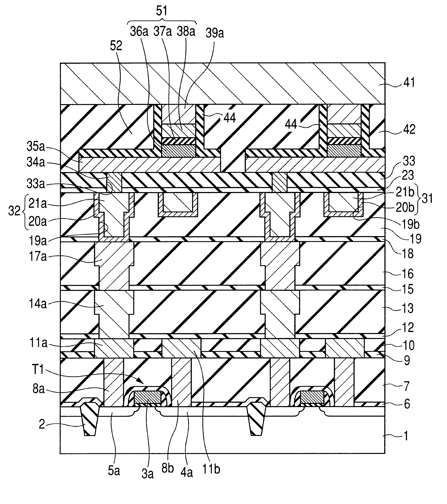
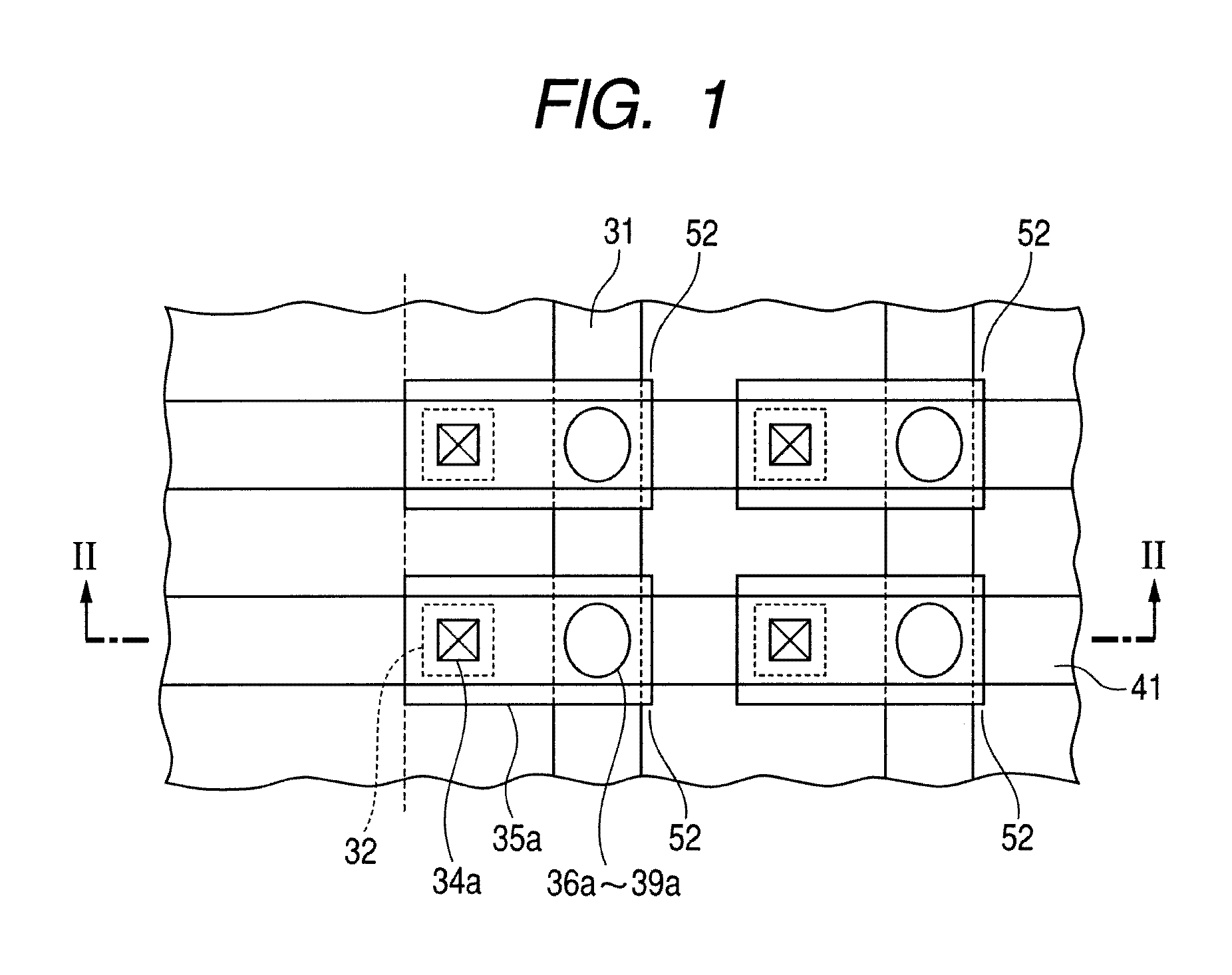
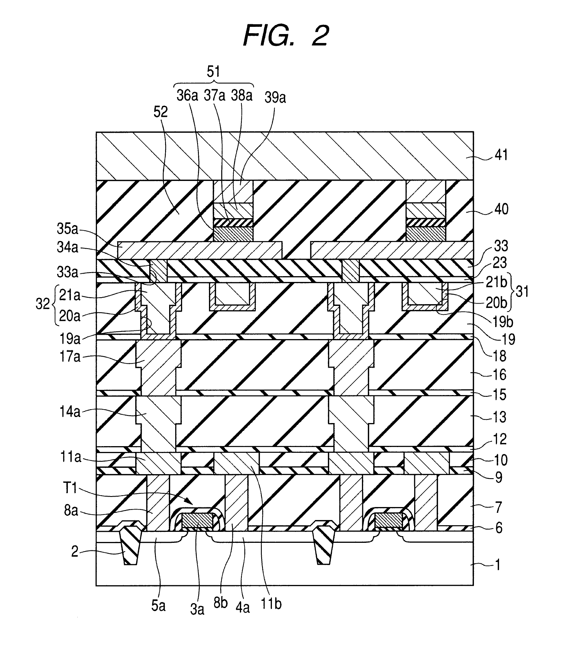
[0065]First, a description will be given to a structure of a memory cell region in a semiconductor device. As shown in FIG. 1, in a memory cell region M, a plurality of digit lines 31 are formed in mutually spaced-apart relation to extend in a direction, and a plurality of bit lines 41 are formed in mutually spaced-apart relation to extend in a direction substantially orthogonal to the direction. At the portions where the digit lines 31 and the bit lines 41 cross each other, magnetic resistor elements 51 are disposed. One ends of the magnetic resistor elements are coupled to the bit lines 41, while the other ends thereof are coupled to the drain regions of element selection transistors (not shown).

[0066]As shown in FIG. 2, each of the element selection transistors T1 has a gate electrode 3a, a source region 4a, and a drain region 5a, and is formed in a surface of an element formation region defined in a semiconductor substrate 1 by an isolation insulating film 2. An etching stopper ...

embodiment 2

[0123]Here, a description will be given to a technique in which the surface of the portion of the interlayer insulating film located in the memory cell region is set by etching at a position lower than that of the surface of the portion of the interlayer insulating film located in the peripheral region.

[0124]In the steps shown in FIG. 4 described above, the etching stopper film 23 is formed so as to cover the interlayer insulating film 19, and the interlayer insulating film 33 is formed over the etching stopper film 23. Then, as shown in FIG. 30, a resist pattern 71 is formed so as to expose the portion of the interlayer insulating film 33 located in the memory cell region M and cover the portion thereof located in the peripheral region P. Using the resist pattern 71 as a mask, the portion of the interlayer insulating film 33 located in the memory cell region M is etched to have the surface thereof set at a position lower than that of the surface of the portion of the interlayer ins...


PUM


Abstract

There are provided a semiconductor device in which short circuit failures in magnetic resistor elements and the like are reduced, and a method of manufacturing the same. An interlayer insulating film in which memory cells are formed is formed such that the upper surface of the portion of the interlayer insulating film located in a memory cell region where the magnetic resistor elements are formed is at a position lower than that of the upper surface of the portion of the interlayer insulating film located in a peripheral region. Another interlayer insulating film is formed so as to cover the magnetic resistor elements. In the another interlayer insulating film, formed are bit lines electrically coupled to the magnetic resistor elements. Immediately below the magnetic resistor elements, formed are digit lines.

Description

CROSS-REFERENCE TO RELATED APPLICATIONS[0001]The disclosure of Japanese Patent Application No. 2009-198181 filed on Aug. 28, 2009 including the specification, drawings and abstract is incorporated herein by reference in its entirety.BACKGROUND OF THE INVENTION[0002]The present invention relates to a semiconductor device and a method of manufacturing the same, and particularly to a semiconductor device including a magnetic resistor element and a method of manufacturing the same.[0003]As a form of a semiconductor device, there is a Magnetic Random Access Memory (MRAM) to which a magnetic resistor element called a Magnetic Tunnel Junction (MTJ) is applied. In the MRAM, the magnetic resistor elements are formed in an array configuration. In each of the magnetic resistor elements, two magnetic layers are stacked with a tunnel insulating film interposed therebetween. According to whether magnetizations in the two magnetic layers are oriented into the same directions or into opposite direc...

Claims


Application Information

Patent Timeline
Patent Type & Authority Applications(United States)
IPC IPC(8): H01L29/82H01L21/18
CPCH01L27/105H01L43/12H01L43/08H01L27/228H10B61/22H10N50/10H10N50/01
Inventor TSUKAMOTO, KEISUKEHIRANO, SHINYAFUJIYAMA, YUICHIROMURATA, TATSUNORI
Owner RENESAS ELECTRONICS CORP
Why Eureka
Try Eureka